ZHCSAW0C February 2013 – October 2016 TLC59731
PRODUCTION DATA.
- 1 特性
- 2 应用范围
- 3 说明
- 4 修订历史记录
- 5 Pin Configuration and Functions
- 6 Specifications
- 7 Parameter Measurement Information
- 8 Detailed Description
- 9 Application and Implementation
- 10Power Supply Recommendations
- 11Layout
- 12器件和文档支持
- 13机械、封装和可订购信息
9 Application and Implementation
NOTE
Information in the following applications sections is not part of the TI component specification, and TI does not warrant its accuracy or completeness. TI’s customers are responsible for determining suitability of components for their purposes. Customers should validate and test their design implementation to confirm system functionality.
9.1 Application Information
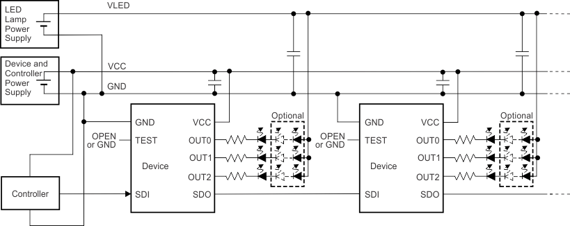
The device is a 3-channel, constant sink current, LED driver. This device can be connected in series to drive many LED lamps with only a few controller ports. Output current control data and PWM control data can be written from the SIN input terminal. The PWM timing reference clock can be supplied from the internal oscillation.
9.2 Typical Application
 Figure 21. Typical Application Circuit Example (No Internal Shunt Regulator Mode)
9.2.1 Design Requirements
For this design example, use Table 4 as the input parameters.
Table 4. Design Parameters
| DESIGN PARAMETER | EXAMPLE VALUE | |||
|---|---|---|---|---|
| VCC Input Voltage Range | 3 V to 5.5 V | |||
| LED Lamp (VLED) Input Voltage Range | 21 V Maximum | |||
| SDI Voltage Range | Low Level = GND, High Level = VCC | |||
9.2.2 Detailed Design Procedure
9.2.2.1 Define Basic Parameters
To begin the design process, a few parameters must be decided:
- Maximum output constant-current value for each color LED lamp
- Maximum LED forward voltage (Vf) and Maximum VLED
- Total LEDs and Cascaded IC Number
9.2.2.2 Grayscale (GS) Data
32-bit GS data packets are sent through single-wire interface for the PWM control of three output channels. Select the GS data of each LED lamp and write the GS data to the register following the signal timing.
9.2.3 Application Curve
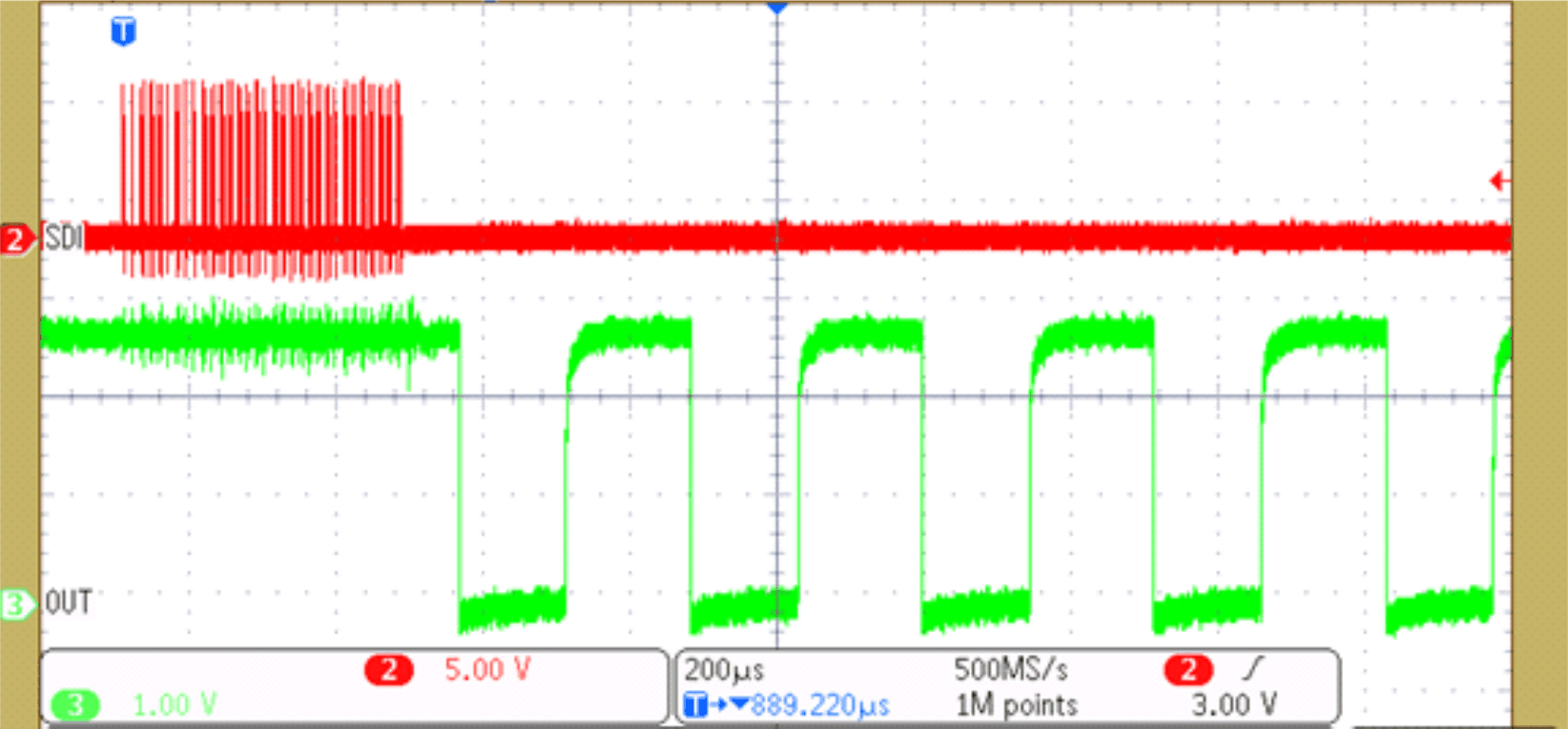
 Figure 22. Output Waveform Without GS Data Latch Input
9.3 System Examples
 Figure 23. Typical Application Circuit Example (No Internal Shunt Regulator Mode)
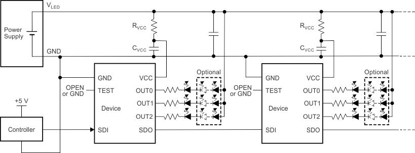
 Figure 24. Typical Application Circuit Example (Internal Shunt Regulator Mode)
9.4 Do's and Don'ts
When the connector pin of the device application printed-circuit-board (PCB) is connected or disconnected to other PCBs, the power must be turned off to avoid device malfunction or failure. Furthermore, designing the connector GND pin to be longer than other pins (as shown in Figure 25) is preferable. This arrangement allows the GND line to either be connected first or disconnected last, which is imperative for proper device function.
 Figure 25. Connector Pin Design Application