SCLS712A March 2009 – June 2015 TLC59211
PRODUCTION DATA.
- 1 Features
- 2 Applications
- 3 Description
- 4 Revision History
- 5 Pin Configuration and Functions
-
6 Specifications
- 6.1 Absolute Maximum Ratings
- 6.2 ESD Ratings
- 6.3 Recommended Operating Conditions
- 6.4 Thermal Information
- 6.5 Electrical Characteristics VCC = 3 V to 3.6 V
- 6.6 Electrical Characteristics VCC = 4.5 V to 5.5 V
- 6.7 Switching Characteristics VCC = 3 V to 3.6 V
- 6.8 Switching Characteristics VCC = 4.5 V to 5.5 V
- 6.9 Typical Characteristics
- 7 Parameter Measurement Information
- 8 Detailed Description
- 9 Application and Implementation
- 10Power Supply Recommendations
- 11Layout
- 12Device and Documentation Support
- 13Mechanical, Packaging, and Orderable Information
11 Layout
11.1 Layout Guidelines
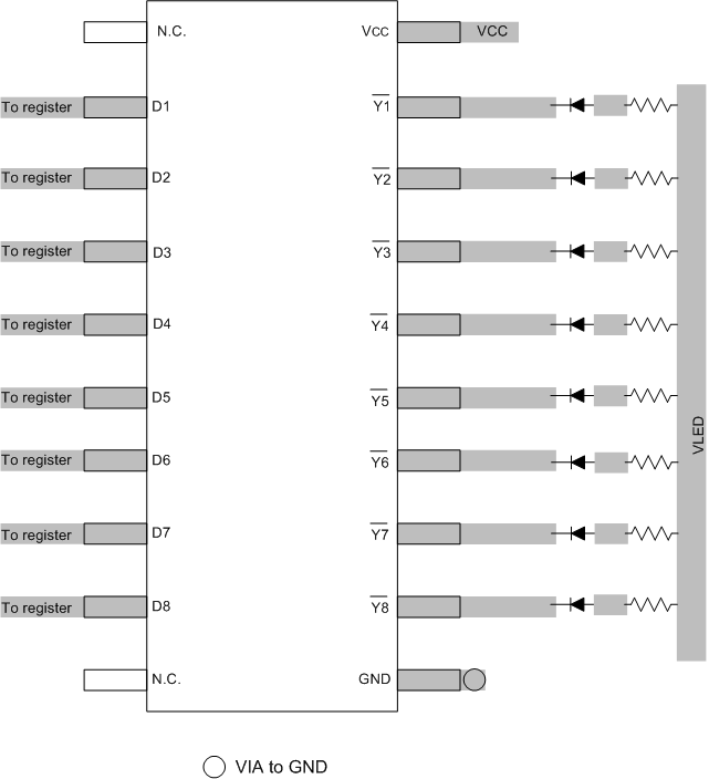
The traces that carry current from the LED cathodes to the OUTx pins must be wide enough to support the current (up to 200 mA).
11.2 Layout Example
 Figure 6. Layout Example Recommendation