SCLS712A March 2009 – June 2015 TLC59211
PRODUCTION DATA.
- 1 Features
- 2 Applications
- 3 Description
- 4 Revision History
- 5 Pin Configuration and Functions
-
6 Specifications
- 6.1 Absolute Maximum Ratings
- 6.2 ESD Ratings
- 6.3 Recommended Operating Conditions
- 6.4 Thermal Information
- 6.5 Electrical Characteristics VCC = 3 V to 3.6 V
- 6.6 Electrical Characteristics VCC = 4.5 V to 5.5 V
- 6.7 Switching Characteristics VCC = 3 V to 3.6 V
- 6.8 Switching Characteristics VCC = 4.5 V to 5.5 V
- 6.9 Typical Characteristics
- 7 Parameter Measurement Information
- 8 Detailed Description
- 9 Application and Implementation
- 10Power Supply Recommendations
- 11Layout
- 12Device and Documentation Support
- 13Mechanical, Packaging, and Orderable Information
8 Detailed Description
8.1 Overview
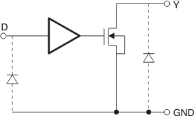
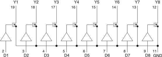
The TLC59211 is an 8-bit parallel LED and solenoid driver designed for 5-V VCC operation. Each channel is individually controlled by its input.
8.2 Functional Block Diagram

8.3 Feature Description
Each of the 8 channels is controlled by its input Dn. When Dn is logic high, the current sink is enabled, output is low. When Dn is logic low, the current sink is disabled, output is pulled high.

1. This symbol is in accordance with ANSI/IEEE Standard 91-1984 and IEC Publication 617-12.
Figure 3. Logic Symbol1