SGLS156F March 2003 – December 2016 TLC3702-Q1
PRODUCTION DATA.
- 1 Features
- 2 Applications
- 3 Description
- 4 Revision History
- 5 Pin Configuration and Functions
- 6 Specifications
- 7 Parameter Measurement Information
- 8 Detailed Description
- 9 Application and Implementation
- 10Power Supply Recommendations
- 11Layout
- 12Device and Documentation Support
- 13Mechanical, Packaging, and Orderable Information
6 Specifications
6.1 Absolute Maximum Ratings
over operating free-air temperature range (unless otherwise noted) (1)| MIN | MAX | UNIT | |||
|---|---|---|---|---|---|
| Supply voltage, VDD (2) | −0.3 | 18 | V | ||
| Differential input voltage, VID(3) | ±18 | V | |||
| Input voltage, VI | −0.3 | VDD | V | ||
| Output voltage, VO | −0.3 | VDD | V | ||
| Input current, II | ±5 | mA | |||
| Output current, IO (each output) | ±20 | mA | |||
| Total supply current into VDD | 40 | mA | |||
| Total current out of GND | 40 | mA | |||
| Continuous total power dissipation | See Thermal Information | ||||
| Operating free-air temperature, TA | −40 | 125 | °C | ||
| Lead temperature 1,6 mm (1/16 inch) from case for 10 seconds | D package | 260 | °C | ||
| PW package | 260 | ||||
| Storage temperature, Tstg | −65 | 150 | °C | ||
(1) Stresses beyond those listed under Absolute Maximum Ratings may cause permanent damage to the device. These are stress ratings only, which do not imply functional operation of the device at these or any other conditions beyond those indicated under Recommended Operating Conditions. Exposure to absolute-maximum-rated conditions for extended periods may affect device reliability.
(2) All voltage values, except differential voltages, are with respect to GND.
(3) Differential voltages are at IN+ with respect to IN−.
6.2 ESD Ratings
| VALUE | UNIT | ||||
|---|---|---|---|---|---|
| V(ESD) | Electrostatic discharge | Human-body model (HBM), per AEC Q100-002(1) | All pins | ±2000 | V |
| Charged-device model (CDM), per AEC Q100-011 | All pins except 1, 4, 5, and 8 | ±500 | |||
| Pins 1, 4, 5, and 8 | ±750 | ||||
(1) AEC Q100-002 indicates that HBM stressing shall be in accordance with the ANSI/ESDA/JEDEC JS-001 specification.
6.3 Recommended Operating Conditions
| MIN | NOM | MAX | UNIT | ||
|---|---|---|---|---|---|
| VDD | Supply voltage | 4 | 5 | 16 | V |
| VIC | Common-mode input voltage | 0 | VDD - 1.5 | V | |
| IOH | High-level output current | –20 | mA | ||
| IOL | Low-level output current | 20 | mA | ||
| TA | Operating free-air temperature | –40 | 125 | °C | |
6.4 Thermal Information
| THERMAL METRIC(1) | TLC3702-Q1 | UNIT | ||
|---|---|---|---|---|
| D (SOIC) | PW (TSSOP) | |||
| 8 PINS | 8 PINS | |||
| RθJA | Junction-to-ambient thermal resistance | 117.7 | 181.1 | °C/W |
| RθJC(top) | Junction-to-case (top) thermal resistance | 63.9 | 49.9 | °C/W |
| RθJB | Junction-to-board thermal resistance | 57.8 | 110.1 | °C/W |
| ψJT | Junction-to-top characterization parameter | 15.3 | 2.4 | °C/W |
| ψJB | Junction-to-board characterization parameter | 57.3 | 108.2 | °C/W |
| RθJC(bot) | Junction-to-case (bottom) thermal resistance | — | — | °C/W |
(1) For more information about traditional and new thermal metrics, see the Semiconductor and IC Package Thermal Metrics application report.
6.5 Electrical Characteristics
at specified operating free-air temperature range, VDD = 5 V (unless otherwise noted). See (2)| PARAMETER | TEST CONDITIONS | TA | MIN | TYP | MAX | UNIT | |
|---|---|---|---|---|---|---|---|
| VIO | Input offset voltage | VDD = 5 V to 10 V, VIC = VICRmin, See (1) |
25°C | 1.2 | 5 | mV | |
| −40°C to +125°C | 10 | ||||||
| IIO | Input offset current | VIC = 2.5 V | 25°C | 1 | pA | ||
| 125°C | 15 | ||||||
| IIB | Input bias current | VIC = 2.5 V | 25°C | 5 | pA | ||
| 125°C | 30 | nA | |||||
| VICR | Common-mode input voltage range | 25°C | 0 to VDD − 1 | V | |||
| −40°C to +125°C | 0 to VDD − 1.5 | ||||||
| CMRR | Common-mode rejection ratio | VIC = VICRmin | 25°C | 84 | dB | ||
| 125°C | 83 | ||||||
| −40°C | 82 | ||||||
| kSVR | Supply-voltage rejection ratio | VDD = 5 V to 10 V | 25°C | 85 | dB | ||
| 125°C | 85 | ||||||
| −40°C | 82 | ||||||
| VOH | High-level output voltage | VID = 1 V, IOH = −4 mA | 25°C | 4.5 | V | ||
| 125°C | 4.2 | ||||||
| VOL | Low-level output voltage | VID = 1 V, IOH = −4 mA | 25°C | 210 | 300 | mV | |
| 125°C | 500 | ||||||
| IDD | Supply current (both comparators) | Outputs low, No load | 25°C | 19 | 40 | µA | |
| −40°C to +125°C | 90 | ||||||
(1) The offset voltage limits given are the maximum values required to drive the output up to 4.5 V or down to 0.3 V.
(2) All characteristics are measured with zero common-mode voltage unless otherwise noted.
6.6 Switching Characteristics
at recommended operating conditions, VDD = 5 V, TA = 25°C (unless otherwise noted)| PARAMETER | TEST CONDITIONS | MIN | TYP | MAX | UNIT | ||
|---|---|---|---|---|---|---|---|
| t(PLH) | Propagation response time, low-to-high-level output (1) | f = 10 kHz, CL = 50 pF |
Overdrive = 2 mV | 4.5 | µs | ||
| Overdrive = 5 mV | 2.7 | ||||||
| Overdrive = 10 mV | 1.9 | ||||||
| Overdrive = 20 mV | 1.4 | ||||||
| Overdrive = 40 mV | 1.1 | ||||||
| VI = 1.4 V step at IN+ | 1.1 | µs | |||||
| t(PHL) | Propagation response time, high-to-low-level output (1) | f = 10 kHz, CL = 50 pF |
Overdrive = 2 mV | 4 | |||
| Overdrive = 5 mV | 2.3 | ||||||
| Overdrive = 10 mV | 1.5 | ||||||
| Overdrive = 20 mV | 0.95 | ||||||
| Overdrive = 40 mV | 0.65 | ||||||
| VI = 1.4 V step at IN+ | 0.15 | ||||||
| tf | Fall time | f = 10 kHz, CL = 50 pF |
Overdrive = 50 mV | 50 | ns | ||
| tr | Rise time | f = 10 kHz, CL = 50 pF |
Overdrive = 50 mV | 125 | ns | ||
(1) Simultaneous switching of inputs causes degradation in output response.
6.7 Typical Characteristics
Table 1. Table of Graphs
| FIGURE | |||
|---|---|---|---|
| VIO | Input offset voltage | Distribution | Figure 1 |
| IIB | Input bias current | vs Free-air temperature | Figure 2 |
| CMRR | Common-mode rejection ratio | vs Free-air temperature | Figure 3 |
| kSVR | Supply-voltage rejection ratio | vs Free-air temperature | Figure 4 |
| VOH | High-level output current | vs Free-air temperature | Figure 5 |
| vs High-level output current | Figure 6 | ||
| VOL | Low-level output voltage | vs Low-level output current | Figure 7 |
| vs Free-air temperature | Figure 8 | ||
| tt | Transition time | vs Load capacitance | Figure 9 |
| Supply current response | vs Time | Figure 10 | |
| Low-to-high-level output response | Low-to-high level output propagation delay time | Figure 11 | |
| High-to-low level output response | High-to-low level output propagation delay time | Figure 12 | |
| tPLH | Low-to-high level output propagation delay time | vs Supply voltage | Figure 13 |
| tPHL | High-to-low level output propagation delay time | vs Supply voltage | Figure 14 |
| IDD | Supply current | vs Frequency | Figure 15 |
| vs Supply voltage | Figure 16 | ||
| vs Free-air temperature | Figure 17 | ||
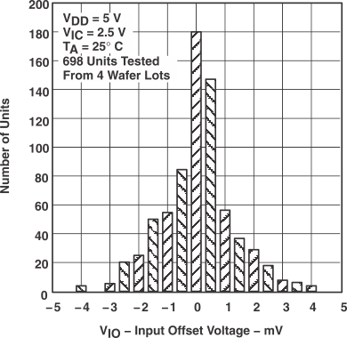 Figure 1. Distribution of Input Offset Voltage
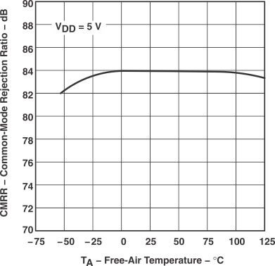 Figure 3. Common-Mode Rejection Ratio vs Free-Air Temperature
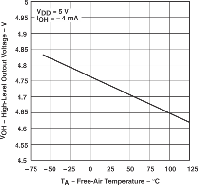 Figure 5. High-Level Output Current vs Free-Air Temperature
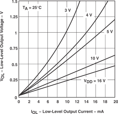 Figure 7. Low-Level Output Voltage vs Low-Level Output Current
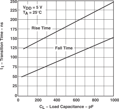 Figure 9. Output Transition Time vs Load Capacitance
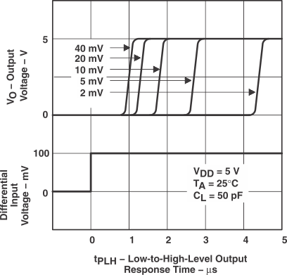 Figure 11. Low-to-High-Level Output Response for Various Input Overdrives
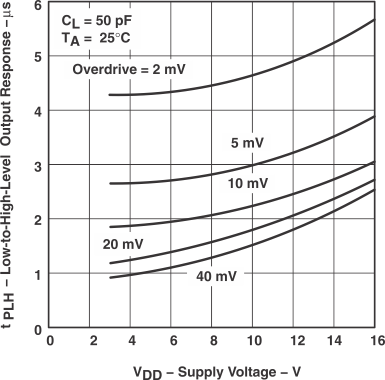 Figure 13. Low-to-High-Level Output Response Time vs Supply Voltage
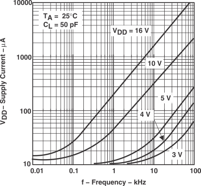 Figure 15. Average Supply Current (per Comparator) vs Frequency
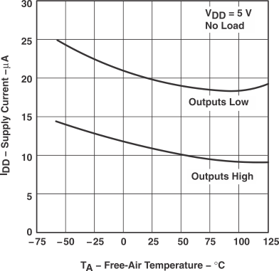 Figure 17. Supply Current vs Free-Air Temperature
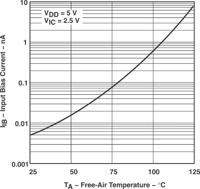 Figure 2. Input Bias Current vs Free-Air Temperature
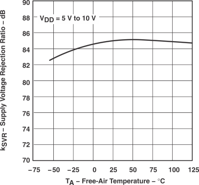 Figure 4. Supply-Voltage Rejection Ratio vs Free-Air Temperature
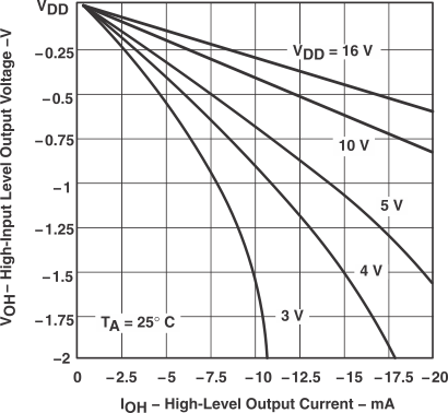 Figure 6. High-Level Output Current vs High-Level Output Current
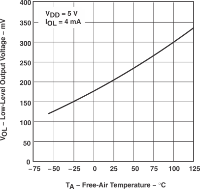 Figure 8. Low-Level Output Voltage vs Free-Air Temperature
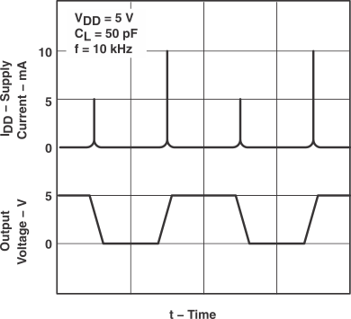 Figure 10. Supply Current Response to an Output Voltage Transition
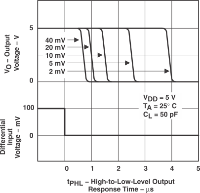 Figure 12. High-to-Low-Level Output Response for Various Input Overdrives
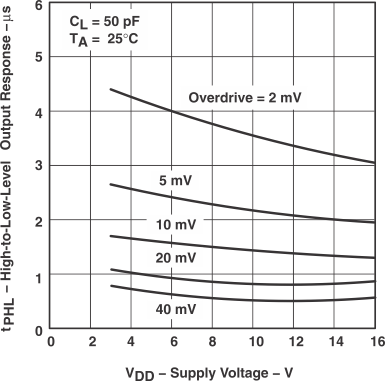 Figure 14. High-to-Low-Level Output Response Time vs Supply Voltage
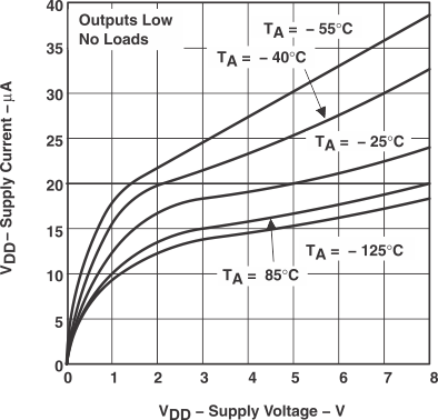 Figure 16. Supply Current vs Supply Voltage