ZHCSJJ4A march   2019  – august 2021 TL7700-SEP

PRODUCTION DATA  

  1. 特性
  2. 应用
  3. 说明
  4. Revision History
  5. Pin Configuration and Functions
  6. Specifications
    1. 6.1 Absolute Maximum Ratings
    2. 6.2 ESD Ratings
    3. 6.3 Recommended Operating Conditions
    4. 6.4 Thermal Information
    5. 6.5 Electrical Characteristics
    6. 6.6 Switching Characteristics
    7. 6.7 Typical Characteristics
  7. Parameter Measurement Information
  8. Detailed Description
    1. 8.1 Overview
    2. 8.2 Functional Block Diagram
    3. 8.3 Feature Description
      1. 8.3.1 Sense-Voltage Setting
      2. 8.3.2 Sense-Voltage Hysteresis Setting
      3. 8.3.3 Output Pulse-Duration Setting
    4. 8.4 Device Functional Modes
  9. Application and Implementation
    1. 9.1 Application Information
    2. 9.2 Typical Application
      1. 9.2.1 Design Requirements
      2. 9.2.2 Detailed Design Procedure
      3. 9.2.3 Application Curve
  10. 10Power Supply Recommendations
  11. 11Layout
    1. 11.1 Layout Guidelines
    2. 11.2 Layout Example
  12. 12Device and Documentation Support
    1. 12.1 接收文档更新通知
    2. 12.2 支持资源
    3. 12.3 Trademarks
    4. 12.4 静电放电警告
    5. 12.5 术语表
  13. 13Mechanical, Packaging, and Orderable Information

封装选项

机械数据 (封装 | 引脚)
散热焊盘机械数据 (封装 | 引脚)
订购信息

Typical Characteristics

Data at high and low temperatures are applicable only within the recommended operating conditions.
GUID-3E9F4BEF-16C9-4A3C-8790-1B965976363A-low.gif
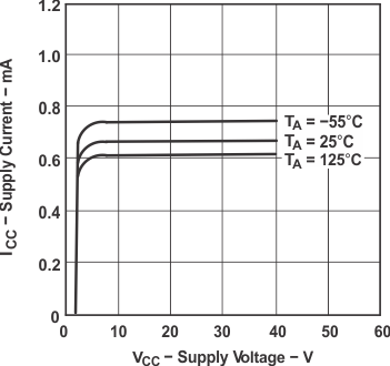
Figure 6-1 Supply Current vs Supply Voltage
GUID-553F7C13-2A50-441A-908A-E7482F06B9DD-low.gif
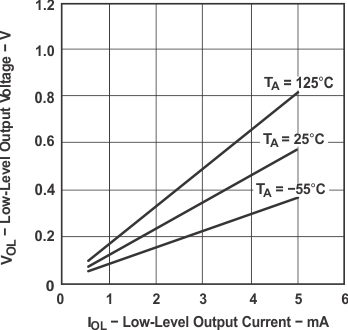
Figure 6-3 VOL vs IOL
GUID-E562AE5B-A999-4A2C-821A-78BFC6AF4FE6-low.gif
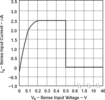
Figure 6-5 Sense Input Current vs Sense Input Voltage
GUID-41851B51-BDD5-4878-A070-B2FB7ED0A5EF-low.gif
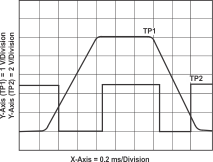
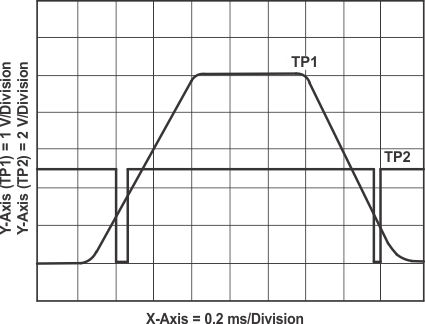
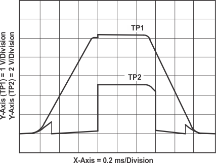
Figure 6-7 VCC vs Output Waveform 1 - See Figure 6-8
GUID-B3614F43-907A-4EEE-BD55-066776EAAF70-low.gif
Figure 6-9 VCC vs Output Waveform 2 - See Figure 6-10
GUID-2E67C6CF-0144-4E47-91B8-B33FDC5EE541-low.gif
Figure 6-11 VCC vs Output Waveform 3 - See Figure 6-12
GUID-676EA0DB-5F6D-4530-87B4-0B3B3A6AD2D6-low.gif
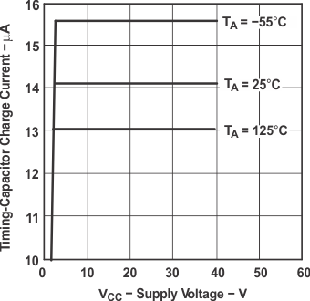
Figure 6-2 Timing Capacitor Charge Current vs Supply Voltage
GUID-68EA4EC3-0E18-42B6-8D0D-3A4626936104-low.gif
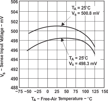
Figure 6-4 Sense Input Voltage vs Temperature
GUID-EBB0EF35-AD90-4E78-9A34-A84AF9F351A2-low.gif
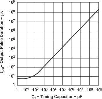
Figure 6-6 Output Pulse Duration vs Timing Capacitor
GUID-D22D327F-7A3D-4AEA-BE6D-35167E55A1A9-low.gif
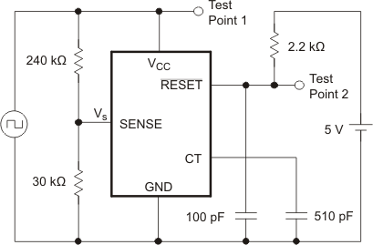
Figure 6-8 VCC vs Output Test Circuit 1
GUID-8599CCBA-7AC6-4268-ADA3-CADA79D4DB3C-low.gif
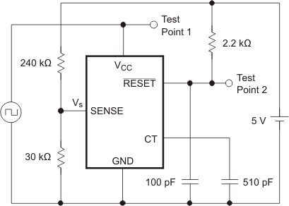
Figure 6-10 VCC vs Output Test Circuit 2
GUID-E04CB81D-B7CD-4AF5-A251-A113AE14E37F-low.gif
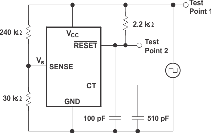
Figure 6-12 VCC vs Output Test Circuit 3