SGLS380H September 2008 – July 2015 TL720M05-Q1
UNLESS OTHERWISE NOTED, this document contains PRODUCTION DATA.
- 1 Features
- 2 Applications
- 3 Description
- 4 Revision History
- 5 Pin Configuration and Functions
- 6 Specifications
- 7 Parameter Measurement Information
- 8 Detailed Description
- 9 Application and Implementation
- 10Power Supply Recommendations
- 11Layout
- 12Device and Documentation Support
- 13Mechanical, Packaging, and Orderable Information
封装选项
请参考 PDF 数据表获取器件具体的封装图。
机械数据 (封装 | 引脚)
- KVU|3
- PWP|20
- KTT|3
散热焊盘机械数据 (封装 | 引脚)
订购信息
6 Specifications
6.1 Absolute Maximum Ratings
over operating free-air temperature range (unless otherwise noted) (1)| MIN | MAX | UNIT | |||
|---|---|---|---|---|---|
| VI | Input voltage(2) | –42 | 45 | V | |
| VO | Output voltage | –1 | 40 | V | |
| TJ | Operating virtual-junction temperature | –40 | 150 | °C | |
| Tstg | Storage temperature | –65 | 150 | °C | |
(1) Stresses beyond those listed under Absolute Maximum Ratings may cause permanent damage to the device. These are stress ratings only, and functional operation of the device at these or any other conditions beyond those indicated under Recommended Operating Conditions is not implied. Exposure to absolute-maximum-rated conditions for extended periods may affect device reliability.
(2) All voltage values are with respect to the network ground terminal.
6.2 ESD Ratings
| VALUE | UNIT | |||||
|---|---|---|---|---|---|---|
| V(ESD) | Electrostatic discharge | Human body model (HBM), per AEC Q100-002(1) | ±6000 | V | ||
(1) AEC Q100-002 indicates HBM stressing is done in accordance with the ANSI/ESDA/JEDEC JS-001 specification.
6.3 Recommended Operating Conditions
over operating free-air temperature range (unless otherwise noted)| MIN | NOM | MAX | UNIT | ||
|---|---|---|---|---|---|
| VI | Input voltage | 5.5 | 42 | V | |
| TA | Operating free-air temperature | –40 | 125 | °C | |
| TJ | Operating virtual-junction temperature | –40 | 150 | °C | |
6.4 Thermal Information
| THERMAL METRIC(1) | TL720M05-Q1 | UNIT | |||
|---|---|---|---|---|---|
| KTT (TO-263) |
KVU (TO-252) |
PWP (HTSSOP) |
|||
| 3 PINS | 3 PINS | 20 PINS | |||
| RθJA | Junction-to-ambient thermal resistance | 34.2 | 45.3 | 39.3 | °C/W |
| RθJC(top) | Junction-to-case (top) thermal resistance | 38.2 | 36.8 | 22.7 | °C/W |
| RθJB | Junction-to-board thermal resistance | 44.9 | 30.8 | 19.1 | °C/W |
| ψJT | Junction-to-top characterization parameter | 6 | 2.8 | 0.6 | °C/W |
| ψJB | Junction-to-board characterization parameter | 44.5 | 30.2 | 18.9 | °C/W |
| RθJC(bot) | Junction-to-case (bottom) thermal resistance | 0.8 | 0.7 | 1.5 | °C/W |
(1) For more information about traditional and new thermal metrics, see the Semiconductor and IC Package Thermal Metrics application report, SPRA953
6.5 Electrical Characteristics
over recommended operating free-air temperature range, VI = 13.5 V, TJ = −40°C to 150°C (unless otherwise noted) (see Figure 13)| PARAMETER | TEST CONDITIONS | MIN | TYP | MAX | UNIT | ||
|---|---|---|---|---|---|---|---|
| VO | Output voltage | IO = 5 mA to 400 mA, VI = 6 V to 28 V | 4.9 | 5 | 5.1 | V | |
| IO = 5 mA to 200 mA, VI = 6 V to 40 V | 4.9 | 5 | 5.1 | ||||
| IO | Output current limit | 450 | 700 | 950 | mA | ||
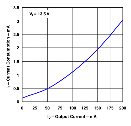
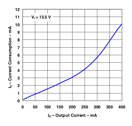
| IQ | Current consumption Iq = II − IO |
IO = 1 mA | TJ = 25°C | 100 | 220 | µA | |
| TJ ≤ 85°C | 100 | 220 | |||||
| IO = 250 mA | 5 | 10 | mA | ||||
| IO = 400 mA | 12 | 22 | |||||
| VDO | Dropout voltage(1) | IO = 300 mA, Vdo = VI − VO | 250 | 500 | mV | ||
| Load regulation | IO = 5 mA to 400 mA | 15 | 30 | mV | |||
| Line regulation | ΔVI = 8 to 32 V, IO = 5 mA | –15 | 5 | 15 | mV | ||
| PSRR | Power-supply ripple rejection | fr = 100 Hz, Vr = 0.5 Vpp | 60 | dB | |||
 |
Temperature output-voltage drift | 0.5 | mV/K | ||||
(1) Measured when the output voltage VO has dropped 100 mV from the nominal value obtained at VI = 13.5 V
6.6 Typical Characteristics


