SGLS380H September 2008 – July 2015 TL720M05-Q1
UNLESS OTHERWISE NOTED, this document contains PRODUCTION DATA.
- 1 Features
- 2 Applications
- 3 Description
- 4 Revision History
- 5 Pin Configuration and Functions
- 6 Specifications
- 7 Parameter Measurement Information
- 8 Detailed Description
- 9 Application and Implementation
- 10Power Supply Recommendations
- 11Layout
- 12Device and Documentation Support
- 13Mechanical, Packaging, and Orderable Information
封装选项
请参考 PDF 数据表获取器件具体的封装图。
机械数据 (封装 | 引脚)
- KVU|3
- PWP|20
- KTT|3
散热焊盘机械数据 (封装 | 引脚)
订购信息
9 Application and Implementation
NOTE
Information in the following applications sections is not part of the TI component specification, and TI does not warrant its accuracy or completeness. TI’s customers are responsible for determining suitability of components for their purposes. Customers should validate and test their design implementation to confirm system functionality.
9.1 Application Information
Based on the end-application, different values of external components can be used. An application can require a larger output capacitor during fast load steps to prevent a reset from occurring. TI recommends a low-ESR ceramic capacitor with a dielectric of type X5R or X7R for better load transient response.
9.2 Typical Application
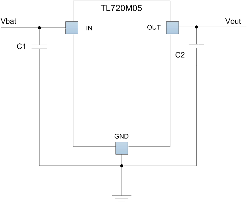
Figure 14 shows typical application circuits for the TL720M05-Q1 device.
 Figure 14. Typical Application Diagram
9.2.1 Design Requirements
For this design example, use the parameters listed in Table 1.
Table 1. Design Parameters
| DESIGN PARAMETER | EXAMPLE VALUE |
|---|---|
| Input voltage range | 4 to 40 V |
| Output voltage | 5 V |
| Output current rating | 400 mA |
| Output capacitor range | 10 to 500 μF |
| Output capacitor ESR range | 1 mΩ to 20 Ω |
9.2.2 Detailed Design Procedure
To begin the design process, determine the following:
- Input voltage range
- Output voltage
- Output current rating
- Output capacitor
9.2.2.1 Thermal Consideration
Calculate the power dissipated by the device according to the following formula:
where
- PT = Total power dissipation of the device.
- IO = output current
- VI = input voltage
- VO = output voltage
After determining the power dissipated by the device, calculate the junction temperature from the ambient temperature and the device thermal impedance.
9.2.3 Application Curves
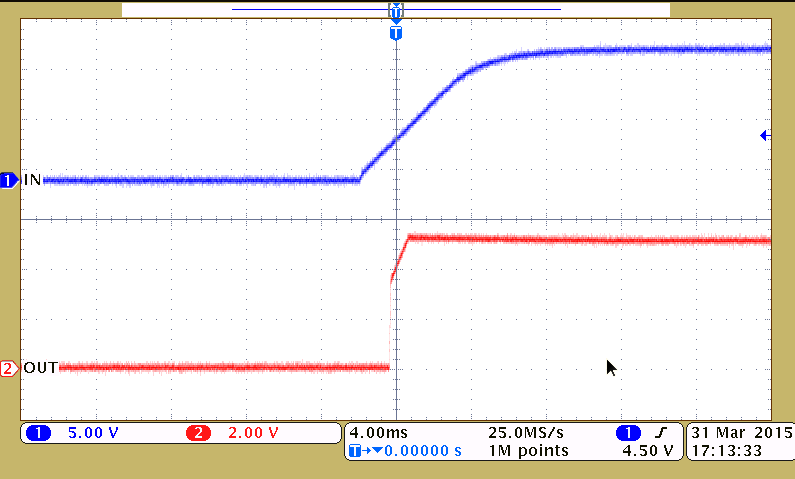
 Figure 15. CH1: Vin, CH2: Vout Power Up Waveform (Load = 50 mA)
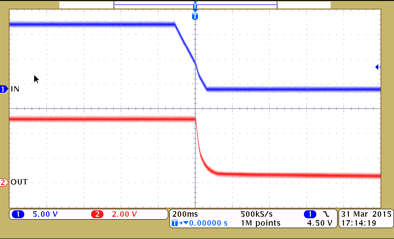
 Figure 16. CH1: Vin, CH2: Vout Power Down Waveform (Load = 50mA)