SLVS038I January 1989 – July 2016 TL2842 , TL2843 , TL2844 , TL2845 , TL3842 , TL3843 , TL3844 , TL3845
PRODUCTION DATA.
- 1 Features
- 2 Applications
- 3 Description
- 4 Revision History
- 5 Pin Configuration and Functions
- 6 Specifications
- 7 Detailed Description
- 8 Application and Implementation
- 9 Power Supply Recommendations
- 10Layout
- 11Device and Documentation Support
- 12Mechanical, Packaging, and Orderable Information
封装选项
请参考 PDF 数据表获取器件具体的封装图。
机械数据 (封装 | 引脚)
- D|8
- D|14
- P|8
散热焊盘机械数据 (封装 | 引脚)
订购信息
6 Specifications
6.1 Absolute Maximum Ratings
over operating free-air temperature range (unless otherwise noted)(1)| MIN | MAX | UNIT | |||
|---|---|---|---|---|---|
| VCC | Supply Voltage(2) | Self limiting | — | ||
| VI | Analog input voltage range, VFB and ISENSE | –0.3 | 6.3 | V | |
| VO | Output Voltage | 35 | V | ||
| VI | Input Voltage, VC and D Package only | 35 | V | ||
| ICC | Supply current | 30 | mA | ||
| IO | Output current | ±1 | A | ||
| error amplifier output sink current | 10 | mA | |||
| TJ | Virtual junction temperature | 150 | °C | ||
| Output energy (capacitive load) | 5 | µJ | |||
| Tstg | Storage temperature | –65 | 150 | °C | |
(1) Stresses beyond those listed under Absolute Maximum Ratings may cause permanent damage to the device. These are stress ratings only, which do not imply functional operation of the device at these or any other conditions beyond those indicated under Recommended Operating Conditions. Exposure to absolute-maximum-rated conditions for extended periods may affect device reliability.
(2) All voltages are with respect to the device GND pin.
6.2 ESD Ratings
| VALUE | UNIT | |||
|---|---|---|---|---|
| V(ESD) | Electrostatic discharge | Human body model (HBM), per ANSI/ESDA/JEDEC JS-001, all pins(1) | 3000 | V |
| Charged device model (CDM), per JEDEC specification JESD22-C101, all pins(2) | 3000 | |||
(1) JEDEC document JEP155 states that 500-V HBM allows safe manufacturing with a standard ESD control process.
(2) JEDEC document JEP157 states that 250-V CDM allows safe manufacturing with a standard ESD control process.
6.3 Recommended Operating Conditions
over operating free-air temperature range (unless otherwise noted)| MIN | TYP | MAX | UNIT | |||
|---|---|---|---|---|---|---|
| VCC and VC(1) | Supply Voltage | 30 | V | |||
| VI, RT/CT | Input Voltage | 0 | 5.5 | V | ||
| VI, VFB and ISENSE | Input Voltage | 0 | 5.5 | V | ||
| VO, OUTPUT | Output voltage | 0 | 30 | V | ||
| VO, POWER GROUND(1) | Output voltage | –0.1 | 1 | V | ||
| ICC | Supply current, externally limited | 25 | mA | |||
| IO | Average output current | 200 | mA | |||
| IO(ref) | Reference output current | –20 | mA | |||
| fOSC | Oscillator frequency | 100 | 500 | kHz | ||
| TA | Operating free-air temperature | TL284x | –40 | 85 | °C | |
| TL384x | 0 | 70 | ||||
(1) These recommended voltages for VC and POWER GROUND apply only to the D package.
6.4 Thermal Information
| THERMAL METRIC(1) | TLx84x | UNIT | |||
|---|---|---|---|---|---|
| D (SOIC) | D (SOIC) | P (PDIP) | |||
| 8 PINS | 14 PINS | 8 PINS | |||
| RθJA | Junction-to-ambient thermal resistance | 97 | 86 | 85 | °C/W |
(1) For more information about traditional and new thermal metrics, see the Semiconductor and IC Package Thermal Metrics application report.
6.5 Electrical Characteristics
over operating free-air temperature range, VCC = 15 V(2), RT = 10 kΩ, CT = 3.3 nF (unless otherwise noted)| PARAMETER | TEST CONDITIONS(1) | TL284x | TL384x | UNIT | ||||||||
|---|---|---|---|---|---|---|---|---|---|---|---|---|
| MIN | TYP(1) | MAX | MIN | TYP(1) | MAX | |||||||
| Reference Section | ||||||||||||
| Output voltage | IO = 1 mA, TA = 25°C | 4.95 | 5 | 5.05 | 4.9 | 5 | 5.1 | V | ||||
| Line regulation | VCC = 12 V to 25 V | 6 | 20 | 6 | 20 | mV | ||||||
| Load regulation | IO = 1 mA to 20 mA | 6 | 25 | 6 | 25 | mV | ||||||
| Temperature coefficient of output voltage | 0.2 | 0.4 | 0.2 | 0.4 | mV/°C | |||||||
| Output voltage with worst-case variation | VCC = 12 V to 25 V, IO = 1 mA to 20 mA | 4.9 | 5.1 | 4.82 | 5.18 | V | ||||||
| Output noise voltage | f = 10 Hz to 10 kHz, TA = 25°C | 50 | 50 | µV | ||||||||
| Output-voltage long-term drift | After 1000 h at TA = 25°C | 5 | 25 | 5 | 25 | mV | ||||||
| Short-circuit output current | –30 | –100 | –180 | –30 | –100 | –180 | mA | |||||
| Oscillator Section | ||||||||||||
| Oscillator frequency(3) | TA = 25°C | 47 | 52 | 57 | 47 | 52 | 57 | kHz | ||||
| Frequency change with supply voltage | VCC = 12 V to 25 V | 2 | 10 | 2 | 10 | Hz/kHz | ||||||
| Frequency change with temperature | 50 | 50 | Hz/kHz | |||||||||
| peak-to-peak amplitude at RT/CT | 1.7 | 1.7 | V | |||||||||
| Error-Amplifier Section | ||||||||||||
| Feedback input voltage | COMP at 2.5 V | 2.45 | 2.50 | 2.55 | 2.42 | 2.50 | 2.58 | V | ||||
| Input bias current | –0.3 | –1 | –0.3 | –2 | µA | |||||||
| Open-loop voltage amplification | VO = 2 V to 4 V | 65 | 90 | 65 | 90 | dB | ||||||
| Gain-bandwidth product | 0.7 | 1 | 0.7 | 1 | MHz | |||||||
| Supply-voltage rejection ratio | VCC = 12 V to 25 V | 60 | 70 | 60 | 70 | dB | ||||||
| Output sink current | VFB, at 2.7 V, COMP at 1.1 V | 2 | 6 | 2 | 6 | mA | ||||||
| Output source current | VFB, at 2.3 V, COMP at 5 V | –0.5 | –0.8 | –0.5 | –0.8 | mA | ||||||
| Hihg-level output voltage | VFB, at 2.3 V, RL = 15 kΩ to GND | 5 | 6 | 5 | 6 | V | ||||||
| Low-level output voltage | VFB, at 2.7 V, RL = 15 kΩ to GND | 0.7 | 1.1 | 0.7 | 1.1 | V | ||||||
| Current-sense Section | ||||||||||||
| Voltage amplification | See(4)(5) | 2.85 | 3 | 3.13 | 2.85 | 3 | 3.15 | V/V | ||||
| Current-sense comparator threshold | COMP at 5 V, see(4) | 0.9 | 1 | 1.1 | 0.9 | 1 | 1.1 | V | ||||
| Supply-voltage rejection ratio | VCC = 12 V to 25 V, see(4) | 70 | 70 | dB | ||||||||
| Input bias current | –2 | –10 | –2 | –10 | µA | |||||||
| Delay time to output | 150 | 300 | 150 | 300 | ns | |||||||
| Output Section | ||||||||||||
| High-level output voltage | IOH = –20 mA | 13 | 13.5 | 13 | 13.5 | V | ||||||
| IOH = –200 mA | 12 | 13.5 | 13 | 13.5 | ||||||||
| Low-level output voltage | IOH = 20 mA | 0.1 | 0.4 | 0.1 | 0.4 | V | ||||||
| IOH = 200 mA | 1.5 | 2.2 | 1.5 | 2.2 | ||||||||
| Rise time | CL = 1 nF, TA = 25°C | 50 | 150 | 50 | 150 | ns | ||||||
| fall time | CL = 1 nF, TA = 25°C | 50 | 150 | 50 | 150 | ns | ||||||
| Undervoltage-Lockout Section | ||||||||||||
| Start threshold voltage | TLx842, TLx844 | 15 | 16 | 17 | 14.5 | 16 | 17.5 | V | ||||
| TLx843, TLx845 | 7.8 | 8.4 | 9 | 7.8 | 8.4 | 9 | ||||||
| Minimum operating voltage after startup | TLx842, TLx844 | 9 | 10 | 11 | 8.5 | 10 | 11.5 | V | ||||
| TLx843, TLx845 | 7 | 7.6 | 8.2 | 7 | 7.6 | 8.02 | ||||||
| Pulse-Width-Modulator Section | ||||||||||||
| Maximum duty cycle | TLx842, TLx843 | 95% | 97% | 100% | 95% | 97% | 100% | |||||
| TLx844, TLx845 | 46% | 48% | 50% | 46% | 48% | 50% | ||||||
| Minimum duty cycle | 0% | 0% | ||||||||||
| Supply Voltage | ||||||||||||
| Start-up current | 0.5 | 1 | 0.5 | 1 | mA | |||||||
| Operating supply current | VFB and ISENSE at 0 V | 11 | 17 | 11 | 17 | mA | ||||||
| Limiting voltage | ICC = 25 mA | 34 | 34 | V | ||||||||
(1) All typical values are at TA = 25°C.
(2) Adjust VCC above the start threshold before setting it to 15 V.
(3) Output frequency equals oscillator frequency for the TLx842 and TLx843. Output frequency is one-half the oscillator frequency for the TLx844 and TLx845.
(4) These parameters are measured at the trip point of the latch, with VFB at 0 V.
(5) Voltage amplification is measured between ISENSE and COMP, with the input changing from 0 V to 0.8 V.
6.6 Typical Characteristics
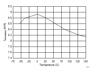 Figure 1. Oscillator Discharge Current
vs
Temperature for VIN = 15 V and VOSC = 2V
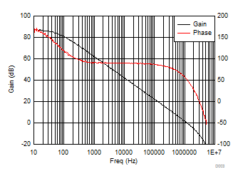 Figure 3. Error Amplifier Open-Loop Gain and Phase
vs
Frequency VCC = 15 V, RL = 100 kΩ, and TA = 25 °C
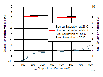 Figure 5. Output Saturation Voltage
 vs
Load Current for VCC = 15 V with 5-ms Input Pulses
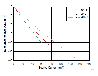 Figure 7. Reference Voltage vs Source Current
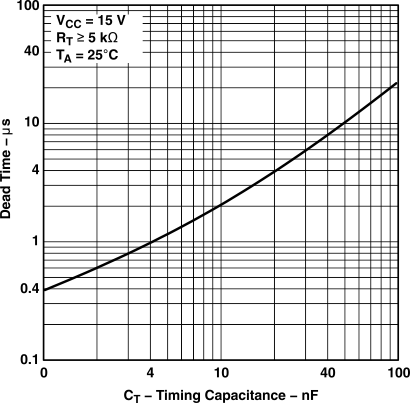 Figure 9. Dead Time vs Timing Capacitance
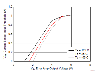 Figure 2. Current Sense Input Threshold
vs
Error Amplifier Output Voltage for VIN = 15 V
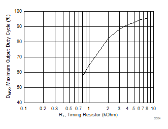 Figure 4. Max Output Duty Cycle
vs
Timing Resistor for VCC = 15, CT = 3.3 nF, TA = 25 °C
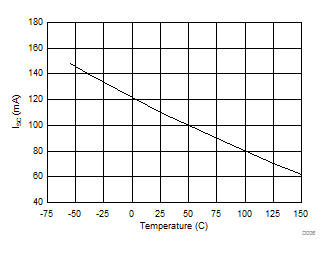 Figure 6. Reference Short Circuit Current
vs
Temperature for VIN = 15 V
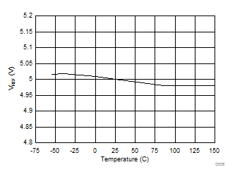 Figure 8. Reference Voltage vs Temperature
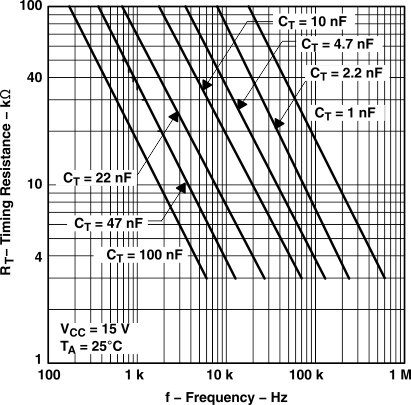 Figure 10. Timing Resistance vs Frequency