SLVS719G June 2008 – January 2015 TL1963A
PRODUCTION DATA.
- 1 Features
- 2 Applications
- 3 Description
- 4 Revision History
- 5 Description (continued)
- 6 Device Comparison Table
- 7 Pin Configuration and Functions
- 8 Specifications
- 9 Detailed Description
- 10Application and Implementation
- 11Power Supply Recommendations
- 12Layout
- 13Device and Documentation Support
- 14Mechanical, Packaging, and Orderable Information
封装选项
机械数据 (封装 | 引脚)
散热焊盘机械数据 (封装 | 引脚)
订购信息
9 Detailed Description
9.1 Overview
The TL1963A-xx series are 1.5-A low-dropout regulators optimized for fast transient response. The devices can supply 1.5 A at a dropout voltage of 340 mV. The low operating quiescent current (1 mA) drops to less than 1 μA in shutdown. In addition to the low quiescent current, the TL1963A-xx regulators incorporate several protection features that make them ideal for use in battery-powered systems. The devices are protected against both reverse input and reverse output voltages. In battery-backup applications where the output can be held up by a backup battery when the input is pulled to ground, the TL1963A-xx acts as if it has a diode in series with its output and prevents reverse-current flow. Additionally, in dual-supply applications where the regulator load is returned to a negative supply, the output can be pulled below ground by as much as (20 V – VIN) and still allow the device to start and operate.
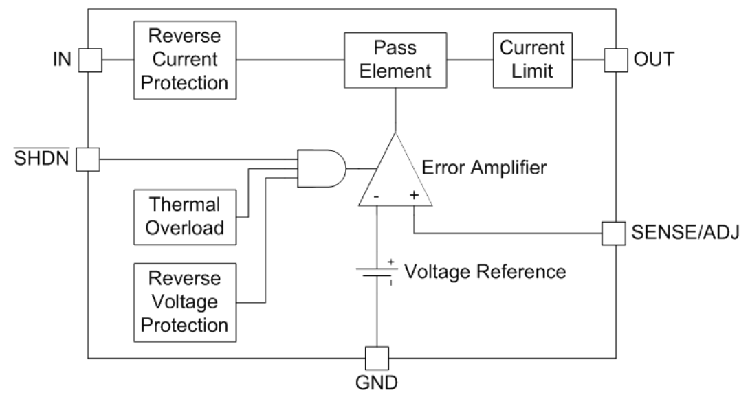
9.2 Functional Block Diagram
9.3 Feature Description
9.3.1 Overload Recovery
Like many IC power regulators, the TL1963A-xx has safe operating area protection. The safe area protection decreases the current limit as input-to-output voltage increases and keeps the power transistor inside a safe operating region for all values of input-to-output voltage. The protection is designed to provide some output current at all values of input-to-output voltage up to the device breakdown.
When power is first turned on, as the input voltage rises, the output follows the input, allowing the regulator to start up into very heavy loads. During start-up, as the input voltage is rising, the input-to-output voltage differential is small, allowing the regulator to supply large output currents. With a high input voltage, a problem can occur wherein removal of an output short does not allow the output voltage to recover. Other regulators also exhibit this phenomenon, so it is not unique to the TL1963A-xx.
The problem occurs with a heavy output load when the input voltage is high and the output voltage is low. Common situations occur immediately after the removal of a short circuit or when the shutdown pin is pulled high after the input voltage has already been turned on. The load line for such a load may intersect the output current curve at two points. If this happens, there are two stable output operating points for the regulator. With this double intersection, the input power supply may need to be cycled down to zero and brought up again to make the output recover.
9.3.2 Output Voltage Noise
The TL1963A-xx regulators have been designed to provide low output voltage noise over the 10-Hz to 100-kHz bandwidth while operating at full load. Output voltage noise is typically 35 nV/√Hz over this frequency bandwidth for the TL1963A (adjustable version). For higher output voltages (generated by using a resistor divider), the output voltage noise is gained up accordingly. This results in RMS noise over the 10-Hz to 100-kHz bandwidth of 14 μVRMS for the TL1963A, increasing to 38 μVRMS for the TL1963A-33.
Higher values of output voltage noise may be measured when care is not exercised with regard to circuit layout and testing. Crosstalk from nearby traces can induce unwanted noise onto the output of the TL1963A-xx. Power-supply ripple rejection must also be considered; the TL1963A-xx regulators do not have unlimited power-supply rejection and pass a small portion of the input noise through to the output.
9.3.3 Protection Features
The TL1963A-xx regulators incorporate several protection features which make them ideal for use in battery-powered circuits. In addition to the normal protection features associated with monolithic regulators, such as current limiting and thermal limiting, the devices are protected against reverse input voltages, reverse output voltages and reverse voltages from output to input.
Current limit protection and thermal overload protection are intended to protect the device against current overload conditions at the output of the device. For normal operation, the junction temperature should not exceed 125°C.
The input of the device withstands reverse voltages of 20 V. Current flow into the device is limited to less than 1 mA (typically less than 100 μA), and no negative voltage appears at the output. The device protects both itself and the load. This provides protection against batteries that can be plugged in backward.
The output of the TL1963A-xx can be pulled below ground without damaging the device. If the input is left open circuit or grounded, the output can be pulled below ground by 20 V. For fixed voltage versions, the output acts like a large resistor, typically 5 kΩ or higher, limiting current flow to typically less than 600 μA. For adjustable versions, the output acts like an open circuit; no current flows out of the pin. If the input is powered by a voltage source, the output sources the short-circuit current of the device and protects itself by thermal limiting. In this case, grounding the SHDN pin turns off the device and stops the output from sourcing the short-circuit current.
The ADJ pin of the adjustable device can be pulled above or below ground by as much as 7 V without damaging the device. If the input is left open circuit or grounded, the ADJ pin acts like an open circuit when pulled below ground and like a large resistor (typically 5 kΩ) in series with a diode when pulled above ground.
In situations where the ADJ pin is connected to a resistor divider that would pull the ADJ pin above its 7-V clamp voltage if the output is pulled high, the ADJ pin input current must be limited to less than 5 mA. For example, a resistor divider is used to provide a regulated 1.5-V output from the 1.21-V reference when the output is forced to 20 V. The top resistor of the resistor divider must be chosen to limit the current into the ADJ pin to less than 5 mA when the ADJ pin is at 7 V. The 13-V difference between OUT and ADJ divided by the 5-mA maximum current into the ADJ pin yields a minimum top resistor value of 2.6 kΩ.
In circuits where a backup battery is required, several different input/output conditions can occur. The output voltage may be held up while the input is either pulled to ground, pulled to some intermediate voltage, or is left open circuit.
When the IN pin of the TL1963A-xx is forced below the OUT pin or the OUT pin is pulled above the IN pin, input current typically drops to less than 2 μA. This can happen if the input of the device is connected to a discharged (low voltage) battery and the output is held up by either a backup battery or a second regulator circuit. The state of the SHDN pin has no effect on the reverse output current when the output is pulled above the input.
9.4 Device Functional Modes
Table 1. Device States
| SHDN | DEVICE STATE |
|---|---|
| H | Regulated Voltage |
| L | Shutdown |