SLVS719G June 2008 – January 2015 TL1963A
PRODUCTION DATA.
- 1 Features
- 2 Applications
- 3 Description
- 4 Revision History
- 5 Description (continued)
- 6 Device Comparison Table
- 7 Pin Configuration and Functions
- 8 Specifications
- 9 Detailed Description
- 10Application and Implementation
- 11Power Supply Recommendations
- 12Layout
- 13Device and Documentation Support
- 14Mechanical, Packaging, and Orderable Information
封装选项
机械数据 (封装 | 引脚)
散热焊盘机械数据 (封装 | 引脚)
订购信息
10 Application and Implementation
NOTE
Information in the following applications sections is not part of the TI component specification, and TI does not warrant its accuracy or completeness. TI’s customers are responsible for determining suitability of components for their purposes. Customers should validate and test their design implementation to confirm system functionality.
10.1 Application Information
This section will highlight some of the design considerations when implementing this device in various applications.
10.1.1 Output Capacitance and Transient Response
The TL1963A-xx regulators are designed to be stable with a wide range of output capacitors. The ESR of the output capacitor affects stability, most notably with small capacitors. A minimum output capacitor of 10 μF with an ESR of 3 Ω or less is recommended to prevent oscillations. Larger values of output capacitance can decrease the peak deviations and provide improved transient response for larger load current changes. Bypass capacitors, used to decouple individual components powered by the TL1963A-xx, increase the effective output capacitor value.
Extra consideration must be given to the use of ceramic capacitors. Ceramic capacitors are manufactured with a variety of dielectrics, each with different behavior over temperature and applied voltage. The most common dielectrics used are Z5U, Y5V, X5R and X7R. The Z5U and Y5V dielectrics are good for providing high capacitances in a small package, but exhibit strong voltage and temperature coefficients. When used with a 5-V regulator, a 10-μF Y5V capacitor can exhibit an effective value as low as 1 μF to 2 μF over the operating temperature range. The X5R and X7R dielectrics result in more stable characteristics and are more suitable for use as the output capacitor. The X7R type has better stability across temperature, while the X5R is less expensive and is available in higher values.
Voltage and temperature coefficients are not the only sources of problems. Some ceramic capacitors have a piezoelectric response. A piezoelectric device generates voltage across its terminals due to mechanical stress, similar to the way a piezoelectric accelerometer or microphone works. For a ceramic capacitor, the stress can be induced by vibrations in the system or thermal transients.
10.2 Typical Applications
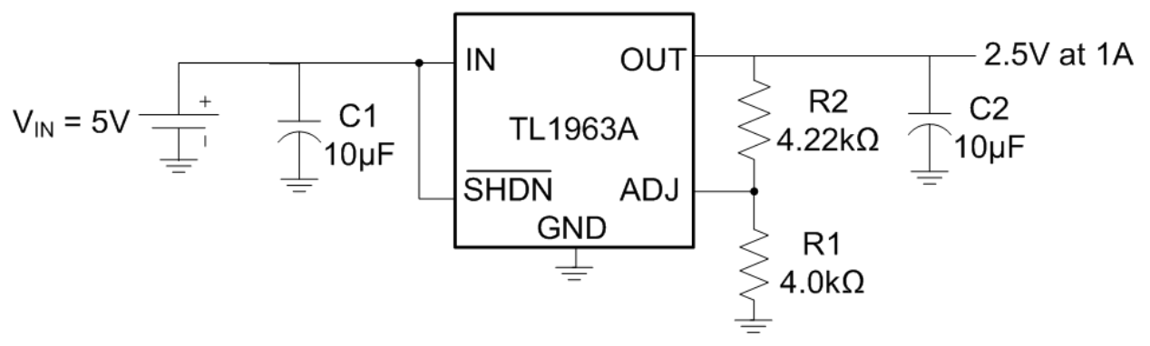
10.2.1 Adjustable Output Operation
NOTE:
All capacitors are ceramic.10.2.1.1 Design Requirements
Table 2. Design Parameters
| DESIGN PARAMETER | EXAMPLE VALUE |
|---|---|
| Input Voltage (VIN) | 5.0 V |
| Output Voltage (VOUT) | 2.5 V |
| Output Current (IOUT) | 0 A to 1 A |
| Load Regulation | 1% |
10.2.1.2 Detailed Design Procedure
The TL1963A has an adjustable output voltage range of 1.21 V to 20 V. The output voltage is set by the ratio of two external resistors R1 and R2 as shown in Figure 30. The device maintains the voltage at the ADJ pin at 1.21 V referenced to ground. The current in R1 is then equal to (1.21 V/R1), and the current in R2 is the current in R1 plus the ADJ pin bias current. The ADJ pin bias current, 3 µA at 25°C, flows through R2 into the ADJ pin. The output voltage can be calculated using Equation 1.
The value of R1 should be less than 4.17 kΩ to minimize errors in the output voltage caused by the ADJ pin bias current. Note that in shutdown the output is turned off, and the divider current is zero. For an output voltage of 2.50 V, R1 will be set to 4.0 kΩ. R2 is then found to be 4.22 kΩ using the equation above.
The adjustable device is tested and specified with the ADJ pin tied to the OUT pin for an output voltage of 1.21 V. Specifications for output voltages greater than 1.21 V are proportional to the ratio of the desired output voltage to 1.21 V: VOUT/1.21 V. For example, load regulation for an output current change of 1 mA to 1.5 A is –2 mV (typ) at VOUT = 1.21 V. At VOUT = 2.50 V, the typical load regulation is:
Figure 33 shows the actual change in output is ~3 mV for a 1A load step. The maximum load regulation at 25 °C is –8 mV. At VOUT = 2.50 V, the maximum load regulation is:
Since 16.53 mV is only 0.7% of the 2.5 V output voltage, the load regulation will meet the design requirements.
10.2.1.2.1 Fixed Operation
The TL1963A-xx can be used in a fixed voltage configuration. The SENSE/ADJ pin should be connected to OUT for proper operation. An example of this is shown in Figure 31. The TL1963A can also be used in this configuration for a fixed output voltage of 1.21 V.
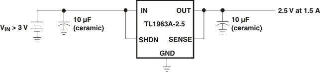 Figure 31. 3.3-V to 2.5-V Regulator
During fixed voltage operation, the SENSE/ADJ pin can be used for a Kelvin connection if routed separately to the load. This allows the regulator to compensate for voltage drop across parasitic resistances (RP) between the output and the load. This becomes more crucial with higher load currents.
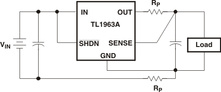 Figure 32. Kelvin Sense Connection
10.2.1.3 Application Curve
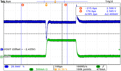 Figure 33. 1-A Load Transient Response (COUT = 10 uF)
10.2.2 Paralleling Regulators for Higher Output Current
NOTE:
All capacitors are ceramic.10.2.2.1 Design Requirements
Table 3. Design Parameters
| DESIGN PARAMETER | EXAMPLE VALUE |
|---|---|
| Input Voltage (VIN) | 6.0 V |
| Output Voltage (VOUT) | 3.3 V |
| Output Current (IOUT) | 3.0 A |
10.2.2.2 Detailed Design Procedure
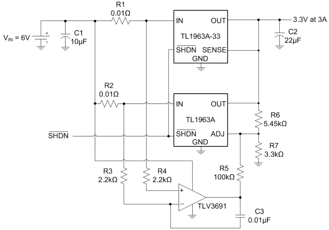
In an application requiring higher output current, an adjustable output regular can be placed in parallel with a fixed output regulator to increase the current capacity. Two sense resistors and a comparator can be used to control the feedback loop of the adjustable regulator in order to balance the current between the two regulators.
In Figure 34 resistors R1 and R2 are used to sense the current flowing into each regulator and should have a very low resistance to avoid unnecessary power loss. R1 and R2 should have the same value and a tolerance of 1% or better so the current is shared equally between the regulators. For this example, a value of 0.01 Ω will be used.
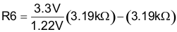
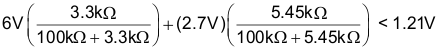
The TLV3691 rail-to-rail nanopower comparator output will alternate between VIN and GND depending on the currents flowing into each of the two regulators. To design this control circuit, begin by looking at the case where the two output currents are approximately equal and the comparator output is low. In this case, the output of the TL1963A should be set the same as the fixed voltage regulator. The TL1963A-33 has a 3.3 V fixed output, so this will be the set point for the adjustable regulator. Begin by selecting a R7 value less than 4.17 kΩ. In this example, 3.3 kΩ will be used. R5 will need to have a high resistance to satisfy Equation 10, for this example 100 kΩ was chosen. Then find the parallel resistance of R5 and R7 since they are both connected from the ADJ pin to GND using Equation 6.
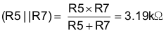
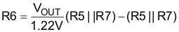
Once the R5 and R7 parallel resistance in calculated, the value for R6 can be found using Equation 7.
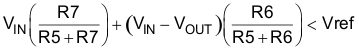
In the case where the TL1963A-33 is sourcing more current than TL1963A, the comparator output will go high. This will lower the voltage at the ADJ pin causing the TL1963A to try and raise the output voltage by sourcing more current. The TL1963A-33 will then react by sourcing less current to try and keep the output from rising. When the current through the TL1963A-33 becomes less than the TL1963A, the comparator output will return to GND. In order for this to happen, Equation 10 must be satisfied:
10.2.2.3 Application Curve
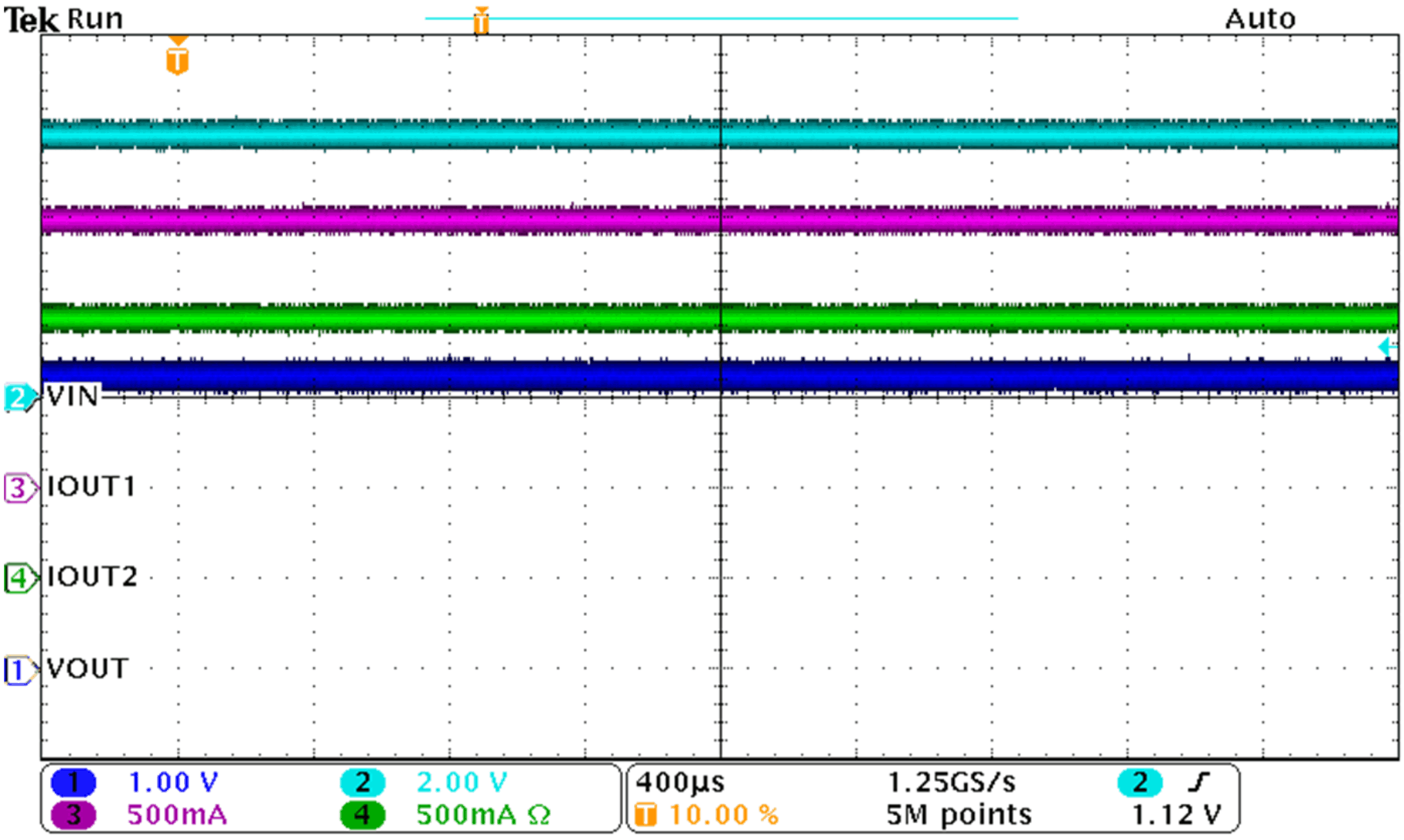 Figure 35. Parallel Regulators Sharing Load Current