ZHCSGR5 September 2017 TIC12400
PRODUCTION DATA.
- 1 特性
- 2 应用
- 3 说明
- 4 修订历史记录
- 5 Pin Configuration and Functions
- 6 Specifications
- 7 Parameter Measurement Information
-
8 Detailed Description
- 8.1 Overview
- 8.2 Functional Block Diagram
- 8.3
Feature Description
- 8.3.1 VS Pin
- 8.3.2 VDD Pin
- 8.3.3 Device Initialization
- 8.3.4 Device Trigger
- 8.3.5 Device Reset
- 8.3.6 VS Under-Voltage (UV) Condition
- 8.3.7 VS Over-Voltage (OV) Condition
- 8.3.8 Switch inputs Settings
- 8.3.9 Interrupt Generation and INT Assertion
- 8.3.10 Temperature Monitor
- 8.3.11 Parity Check And Parity Generation
- 8.3.12 Cyclic Redundancy Check (CRC)
- 8.4 Device Functional Modes
- 8.5 Programming
- 8.6
Register Maps
- 8.6.1 DEVICE_ID register (Offset = 1h) [reset = 20h]
- 8.6.2 INT_STAT Register (Offset = 2h) [reset = 1h]
- 8.6.3 CRC Register (Offset = 3h) [reset = FFFFh]
- 8.6.4 IN_STAT_MISC Register (Offset = 4h) [reset = 0h]
- 8.6.5 IN_STAT_COMP Register (Offset = 5h) [reset = 0h]
- 8.6.6 IN_STAT_ADC0 Register (Offset = 6h) [reset = 0h]
- 8.6.7 IN_STAT_ADC1 Register (Offset = 7h) [reset = 0h]
- 8.6.8 IN_STAT_MATRIX0 Register (Offset = 8h) [reset = 0h]
- 8.6.9 IN_STAT_MATRIX1 Register (Offset = 9h) [reset = 0h]
- 8.6.10 ANA_STAT0 Register (Offset = Ah) [reset = 0h]
- 8.6.11 ANA_STAT1 Register (Offset = Bh) [reset = 0h]
- 8.6.12 ANA_STAT2 Register (Offset = Ch) [reset = 0h]
- 8.6.13 ANA_STAT3 Register (Offset = Dh) [reset = 0h]
- 8.6.14 ANA_STAT4 Register (Offset = Eh) [reset = 0h]
- 8.6.15 ANA_STAT5 Register (Offset = Fh) [reset = 0h]
- 8.6.16 ANA_STAT6 Register (Offset = 10h) [reset = 0h]
- 8.6.17 ANA_STAT7 Register (Offset = 11h) [reset = 0h]
- 8.6.18 ANA_STAT8 Register (Offset = 12h) [reset = 0h]
- 8.6.19 ANA_STAT9 Register (Offset = 13h) [reset = 0h]
- 8.6.20 ANA_STAT10 Register (Offset = 14h) [reset = 0h]
- 8.6.21 ANA_STAT11 Register (Offset = 15h) [reset = 0h]
- 8.6.22 ANA_STAT12 Register (Offset = 16h) [reset = 0h]
- 8.6.23 CONFIG Register (Offset = 1Ah) [reset = 0h]
- 8.6.24 IN_EN Register (Offset = 1Bh) [reset = 0h]
- 8.6.25 CS_SELECT Register (Offset = 1Ch) [reset = 0h]
- 8.6.26 WC_CFG0 Register (Offset = 1Dh) [reset = 0h]
- 8.6.27 WC_CFG1 Register (Offset = 1Eh) [reset = 0h]
- 8.6.28 CCP_CFG0 Register (Offset = 1Fh) [reset = 0h]
- 8.6.29 CCP_CFG1 Register (Offset = 20h) [reset = 0h]
- 8.6.30 THRES_COMP Register (Offset = 21h) [reset = 0h]
- 8.6.31 INT_EN_COMP1 Register (Offset = 22h) [reset = 0h]
- 8.6.32 INT_EN_COMP2 Register (Offset = 23h) [reset = 0h]
- 8.6.33 INT_EN_CFG0 Register (Offset = 24h) [reset = 0h]
- 8.6.34 INT_EN_CFG1 Register (Offset = 25h) [reset = 0h]
- 8.6.35 INT_EN_CFG2 Register (Offset = 26h) [reset = 0h]
- 8.6.36 INT_EN_CFG3 Register (Offset = 27h) [reset = 0h]
- 8.6.37 INT_EN_CFG4 Register (Offset = 28h) [reset = 0h]
- 8.6.38 THRES_CFG0 Register (Offset = 29h) [reset = 0h]
- 8.6.39 THRES_CFG1 Register (Offset = 2Ah) [reset = 0h]
- 8.6.40 THRES_CFG2 Register (Offset = 2Bh) [reset = 0h]
- 8.6.41 THRES_CFG3 Register (Offset = 2Ch) [reset = X]
- 8.6.42 THRES_CFG4 Register (Offset = 2Dh) [reset = X]
- 8.6.43 THRESMAP_CFG0 Register (Offset = 2Eh) [reset = 0h]
- 8.6.44 THRESMAP_CFG1 Register (Offset = 2Fh) [reset = 0h]
- 8.6.45 THRESMAP_CFG2 Register (Offset = 30h) [reset = 0h]
- 8.6.46 Matrix Register (Offset = 31h) [reset = 0h]
- 8.6.47 Mode Register (Offset = 32h) [reset = 0h]
- 8.7 Programming Guidelines
- 9 Application and Implementation
- 10Power Supply Recommendations
- 11Layout
- 12器件和文档支持
- 13机械、封装和可订购信息
8 Detailed Description
8.1 Overview
The TIC12400 is an advanced 24-input Multiple Switch Detection Interface (MSDI) device designed to detect external mechanical switches status in an industrial system by acting as an interface between the switches and the low-voltage microcontroller. The TIC12400 is an integrated solution that replaces many discrete components and provides integrated protection, input serialization, and system wake-up capability.
The device monitors 14 switches to GND and 10 additional switches that can be programmed to be connected to either GND or VSUPPLY. It features SPI interface to report individual switch status and provides programmability to control the device operation. The TIC12400 features a 10-bit ADC, which is useful to monitor analog inputs, such as resistor coded switches, that have multiple switching positions. To monitor only digital switches, an integrated comparator can be used instead to monitor the input status. The device has 2 modes of operation: continuous mode and polling mode. The polling mode is a low-power mode that can be activated to reduce current drawn in the system by only turning on the wetting current for a small duty cycle to detect switch status changes. An interrupt is generated upon detection of switch status change and it can be used to wake up the microcontroller to bring the entire system back to operation.
8.2 Functional Block Diagram
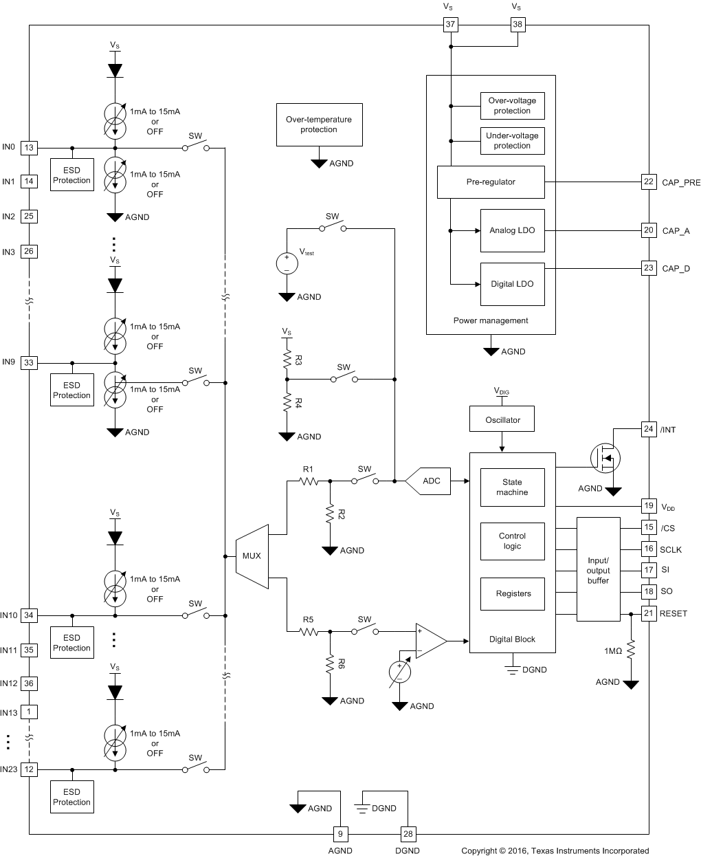
8.3 Feature Description
8.3.1 VS Pin
The VS supply provides power to the entire chip and the TIC12400 is designed to operate with VS ranging from 6.5 V to 35 V.
8.3.2 VDD Pin
The VDD supply is used to determine the logic level on the SPI communication interface, source the current for the SO driver, and sets the pull-up voltage for the CS pin. It can also be used as a possible external pull-up supply for the INT pin in addition to the VS and it shall be connected to a 3 V to 5.5 V logic supply. Removing VDD from the device disables SPI communications, but does not reset the register configurations.
8.3.3 Device Initialization
When the device is powered up for the first time, the condition is called Power-On Reset (POR), which sets the registers to their default values and initializes the device state machine. The internal POR controller holds the device in a reset condition until VS has reached VPOR_R, at which the reset condition is released with the device registers and state machine initialized to their default values. After the initialization process is completed, the INT pin is asserted low to notify the microcontroller, and the register bit POR in the INT_STAT register is asserted to logic 1. The SPI flag bit POR is also asserted at the SPI output (SO).
During device initialization, some factory settings are programmed into the device to allow accurate device operation. The device performs a self-check after the device is programmed to ensure correct settings are loaded. If the self-check returns an error, the CHK_FAIL bit in the INT_STAT register will be flagged to logic 1 along with the POR bit. If this very unlikely event occurs, the microcontroller is recommended to initiate software reset (see section Software Reset) to re-initialize the device to allow the correct settings to be re-programmed.
8.3.4 Device Trigger
After device initialization, the TIC12400 is ready to be configured. The microcontroller can use SPI commands to program desired settings to the configuration registers. Once the device configuration is completed, the microcontroller is required to set the bit TRIGGER in the CONFIG register to logic 1 in order to activate wetting current and start external switch monitoring.
After the switch monitoring starts, the configuration registers turn into read-only registers (with the exception of the TRIGGER, CRC_T, and RESET bits in the CONFIG register and all bits in the CCP_CFG1 register). If at any time the device setting needs to be re-configured, the microcontroller is required to first set the bit TRIGGER in the CONFIG register to logic 0 to stop wetting current and switch monitoring. The microcontroller can then program configuration registers to the desired settings. Once the re-configuration is completed, the microcontroller can set the TRIGGER bit back to logic 1 to re-start switch monitoring.
Note the cyclic redundancy check (CRC) feature stays accessible during switch monitoring, which allows the microcontroller to verify device settings at all time. Refer to section Cyclic Redundancy Check (CRC) for more details of the CRC feature.
8.3.5 Device Reset
There are 3 ways to reset the TIC12400 and re-initialize all registers to their default values:
8.3.5.1 VS Supply POR
The device is turned off and all register contents are lost if the VS voltage drops below VPOR_F. To turn the device back on, the VS voltage must be raised back above VPOR_R, as illustrated in Figure 12. The device then starts the initialization process as described in section Device Initialization .
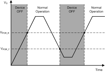 Figure 12. VS is Lowered Below The POR threshold, Then Ramped Back Up To Complete A POR Cycle
8.3.5.2 Hardware Reset
Microcontroller can toggle the RESET pin to perform a hardware reset to the device. The RESET pin is internally pulled-down via a 1MΩ resistor and must be kept low for normal operation. When the RESET pin is toggled high, the device enters the reset state with most of the internal blocks turned off and consumes very little current of IS_RESET. Switch monitoring and SPI communications are stopped in the reset state, and all register contents are cleared. When RESET pin is toggled back low, all the registers are set to their default values and the device state machine is re-initialized, similar to a POR event. When the re-initialization process is completed, the INT pin is asserted low, and the interrupt register bit POR and the SPI status flag POR are both asserted to notify the microcontroller that the device has completed the reset process.
Note in order to successfully reset the device, the RESET pin needs to be kept high for a minimum duration of tRESET. The pin is required to be driven with a stable input (below VRESET_L for logic low or above VRESET_H for logic H) to prevent the device from accidental reset.
8.3.5.3 Software Reset
In addition to hardware reset, the microcontroller can also issue a SPI command to initiate software reset. This is triggered by setting the RESET bit in the register CONFIG to logic 1, which re- initialized the device with all registers set to their default value. When the re-initialization process is completed, the INT pin is asserted low, and the interrupt register bit POR and the SPI status flag POR are both asserted to notify the microcontroller that the device has completed the reset process.
8.3.6 VS Under-Voltage (UV) Condition
During normal operation of a typical 12 V system, the VS voltage is usually quite stable and stays well above 12 V. However, the VS voltage might drops temporarily during certain operations. If the VS voltage drops below VUV_F, the TIC12400 enters the under-voltage (UV) condition since there is not enough voltage headroom for the device to accurately generate wetting currents. The following describes the behavior of the TIC12400 under UV condition:
- All current sources/sinks de-activate and switch monitoring stops.
- Interrupt is generated by asserting the INT pin low and the bit UV in the interrupt register (INT_STAT) is flagged to logic 1. The bit UV_STAT is asserted to logic 1 in the register IN_STAT_MISC. The OI SPI flag is asserted during any SPI transactions. The INT pin is released and the interrupt register (INT_STAT) is cleared on the rising edge of CS provided the interrupt register has been read during the SPI transaction.
- SPI communication stays active, and all register settings say intact without resetting. Previous switch status, if needed, can be retrieved without any interruption.
- The device continues to monitor the VS voltage, and the UV condition sustains if the VS voltage continues to stay below VUV_R. No further interrupt is generated once cleared.
Note the device resets as described in section VS Supply POR if the VS voltage drops below VPOR_F, .
When the VS voltage rises above VUV_R, the INT pin is asserted low to notify the microcontroller that the UV condition no longer exists. The UV bit in the register INT_STAT is flagged to logic 1 and the bit UV_STAT bit is de-asserted to logic 0 in the register IN_STAT_MISC to reflect the clearance of the UV condition. The device resumes operation using current register settings (regardless of the INT pin and SPI communication status) with polling restarted from the first enabled channel. The Switch State Change (SSC) interrupt is generated at the end of the first polling cycle and the detected switch status becomes the baseline switch status for subsequent polling cycles. The content of the INT_STAT register, once read by the microcontroller, is cleared, and the INT pin is released afterwards. .
The following diagram describes the TIC12400 operation at various different VS voltages. If the VS voltage stays above VUV_F (Case 1), the device stays in normal operation. If the VS voltage drops below VUV_F but stays above VPOR_F (Case 2), the device enters the UV condition. If VS voltage drops below VPOR_F (Case 3), the device resets and all register settings are cleared. The microcontroller is then required to re-program all the configuration registers in order to resume normal operation after the VS voltage recovers.
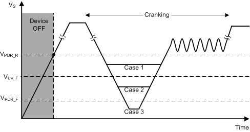 Figure 13. TIC12400 Operation At Various VS Voltage Levels
8.3.7 VS Over-Voltage (OV) Condition
If VS voltage rises above VOV_R, the TIC12400 enters the over-voltage (OV) condition to prevent damage to internal structures of the device on the VS and INx pins. The following describes the behavior of the TIC12400 under OV condition:
- All current sources/sinks de-activate and switch monitoring stops.
- Interrupt is generated by asserting the INT pin low and the bit OV in the interrupt register (INT_STAT) is flagged to logic 1. The bit OV_STAT is asserted to logic 1 in the register IN_STAT_MISC. The OI SPI flag is asserted during any SPI transactions. The INT pin is released and the interrupt register (INT_STAT) is cleared on the rising edge of CS provided the interrupt register has been read during the SPI transaction.
- SPI communication stays active, and all register settings say intact without resetting. Previous switch status, if needed, can be retrieved without any interruption.
- The device continues to monitor the VS voltage, and the OV condition sustains if the VS voltage continues to stays above VOV_R- VOV_HYST. No further interrupt is generated once cleared.
When the VS voltage drops below VOV_R- VOV_HYST, the INT pin is asserted low to notify the microcontroller that the over-voltage condition no longer exists. The OV bit in the register INT_STAT is flagged to logic 1 and the bit OV_STAT bit is de-asserted to logic 0 in the register IN_STAT_MISC to reflect the clearance of the OV condition. The device resumes operation using current register settings (regardless of the INT pin and SPI communication status) with polling restarted from the first enabled channel. The Switch State Change (SSC) interrupt is generated at the end of the first polling cycle and the detected switch status becomes the baseline status for subsequent polling cycles. The content of the INT_STAT register, once read by the microcontroller, is cleared, and the INT pin is released afterwards.
8.3.8 Switch inputs Settings
IN0 to IN23 are inputs connected to external mechanical switches. All the inputs can sustain up to 40 V without being damaged. The switch status of each input, whether open or closed, is indicated by the status registers. Table 1 below describe various settings that can be configured for each input. Note some settings are shared between multiple inputs and it is required to first stop device operation by setting the TRIGGER bit low in the register CONFIG before making any configuration changes, as described in Device Trigger.
Table 1. TIC12400 Wetting Current and Threshold Setting Details
| Input | Threshold | Wetting Current | Current Source (CSO) / Current Sink (CSI) | Supported Switch Type | ||
|---|---|---|---|---|---|---|
| Comparator Input Mode | ADC Input Mode | |||||
| IN0 | THRES_COMP_IN0_IN3 | THRES0 to THRES7 | THRES_COM | WC_IN0_IN1 | CSO CSI |
Switch to GND Switch to VSUPPLY |
| IN1 | THRES0 to THRES7 | CSO CSI |
Switch to GND Switch to VSUPPLY |
|||
| IN2 | THRES0 to THRES7 | WC_IN2_IN3 | CSO CSI |
Switch to GND Switch to VSUPPLY |
||
| IN3 | THRES0 to THRES7 | CSO CSI |
Switch to GND Switch to VSUPPLY |
|||
| IN4 | THRES_COMP_IN4_IN7 | THRES0 to THRES7 | WC_IN4 | CSO CSI |
Switch to GND Switch to VSUPPLY |
|
| IN5 | THRES0 to THRES7 | WC_IN5 | CSO CSI |
Switch to GND Switch to VSUPPLY |
||
| IN6 | THRES0 to THRES7 | WC_IN6_IN7 | CSO CSI |
Switch to GND Switch to VSUPPLY |
||
| IN7 | THRES0 to THRES7 | CSO CSI |
Switch to GND Switch to VSUPPLY |
|||
| IN8 | THRES_COMP_IN8_IN11 | THRES0 to THRES7 | WC_IN8_IN9 | CSO CSI |
Switch to GND Switch to VSUPPLY |
|
| IN9 | THRES0 to THRES7 | CSO CSI |
Switch to GND Switch to VSUPPLY |
|||
| IN10 | THRES0 to THRES7 | WC_IN10 | CSO | Switch to GND | ||
| IN11 | THRES0 to THRES7 | WC_IN11 | CSO | Switch to GND | ||
| IN12 | THRES_COMP_IN12_IN15 | THRES2A THRES2B |
WC_IN12_13 | CSO | Switch to GND | |
| IN13 | THRES2A THRES2B |
CSO | Switch to GND | |||
| IN14 | THRES2A THRES2B |
WC_IN14_15 | CSO | Switch to GND | ||
| IN15 | THRES2A THRES2B |
CSO | Switch to GND | |||
| IN16 | THRES_COMP_IN16_IN19 | THRES2A THRES2B |
WC_IN16_17 | CSO | Switch to GND | |
| IN17 | THRES2A THRES2B |
CSO | Switch to GND | |||
| IN18 | THRES3A THRES3B THRES3C |
WC_IN18_19 | CSO | Switch to GND | ||
| IN19 | THRES3A THRES3B THRES3C |
CSO | Switch to GND | |||
| IN20 | THRES_COMP_IN20_IN23 | THRES3A THRES3B THRES3C |
WC_IN20_21 | CSO | Switch to GND | |
| IN21 | THRES3A THRES3B THRES3C |
CSO | Switch to GND | |||
| IN22 | THRES3A THRES3B THRES3C |
WC_IN22 | CSO | Switch to GND | ||
| IN23 | THRES3A THRES3B THRES3C THRES8 THRES9 |
WC_IN23 | CSO | Switch to GND | ||
8.3.8.1 Input Current Source/Sink Selection
Among the 24 inputs, IN10 to IN23 are intended for monitoring only ground-connected switches and are connected to current sources. IN0 to IN9 can be programmed to monitor either ground-connected switches or supply-connected switches by configuring the CS_SELECT register. The default configuration of the IN0-IN9 inputs after POR is to monitor ground-connected switches (current sources are selected). To set an input to monitor supply-connected switches, set the corresponding bit to logic 1.
8.3.8.2 Input Mode Selection
The TIC12400 has a built-in ADC and a comparator that can be used to monitor resistor coded switches or digital switches. Digital switch inputs have only two states, either open or closed, and can be adequately detected by a comparator. Resistor coded switches may have multiple positions that need to be detected, and an ADC is appropriate to monitor the different states. Each input of the TIC12400 can be individually programmed to use either a comparator or an ADC by configuring the appropriate bits in theMODE register depending on the knowledge of the external switch connections. The benefit of using a comparator instead of an ADC to monitor digital switches is its reduced polling time, which translates to overall power saving when the device operates in the low-power polling mode.
Comparator input mode is selected by default for all enabled inputs upon device reset.
8.3.8.3 Input Enable Selection
The TIC12400 provides switch status monitoring for up to 24 inputs, but there might be circumstances in which not all inputs need to be constantly monitored. The microcontroller may choose to enable/disable monitoring of certain inputs by configuring the IN_EN register. Setting the corresponding bit to logic 0 to de-activates the wetting current source/sink and stops switch status monitoring for the input. Disabling monitoring of unused inputs reduce overall power consumption of the device.
All inputs are disabled by default upon device reset.
8.3.8.4 Thresholds Adjustment
When an input is configured as comparator input mode, the threshold level for interrupt generation of can be programmed by setting the THRES_COMP register. The threshold level settings can be set to for each individual input groups and each group consist of 4 inputs. Four threshold levels are available: 2V, 2.7V, 3V, and 4V.
When an input is configured as ADC input mode, the threshold level for interrupt generation can be configured, up to 1023 different levels, by setting the THRES_CFG1 to THRES_CFG2 registers. One threshold level can be programmed individually for each of the input from IN0 to IN11. Additionally, one common threshold, shared between inputs IN0 to IN11, can be programmed by configuring the THRES_COM bits in register MATRIX. The common threshold acts independently from the threshold THRES0 to THRES7. Inputs IN12 to IN17 use 2 preset threshold levels (THRES2A and THRES2B). Inputs 18 to 22 use 3 preset threshold levels (THRES3A, THRES3B, and THRES3C). Input 23 uses 5 preset threshold levels (THRES3A, THRES3B, THRES3C, THRES8 and THRES9).
When multiple threshold settings are used for ADC inputs, the thresholds levels needs to be configured properly. Use the rules below (see Table 2) when setting up the threshold levels:
Table 2. Proper Threshold Configuration For ADC Inputs
| Input | Proper Threshold Configuration |
|---|---|
| IN12 to IN17 | THRES2B ≥ THRES2A |
| IN18 to IN22 | THRES3C ≥ THRES3B ≥ THRES3A |
| IN23 | THRES9 ≥ THRES8 ≥ THRES3C ≥ THRES3B ≥ THRES3A |
Caution should be used when setting up the threshold for switches that are connected externally to the supply as there are finite voltage drop (as high as VCSI_DROP for 10mA and 15mA settings) across the current sinks. Therefore, even for an open switch, then voltage on the INx pin can be as high as VCSI_DROP and the detection threshold shall be configured above it. It shall also be noted that a lower wetting current sink setting might not be stronger enough to pull the INx pin close to ground in the presence of a leaky open external switch, as illustrated in the diagram below (see Figure 14). In this example, the external switch, although in the open state, has large leakage current and can be modelled as an equivalent resistor (RDIRT) of 5kΩ. The 2mA current sink is only able to pull the INx pin voltage down to 2V, even the switch is in the open state.
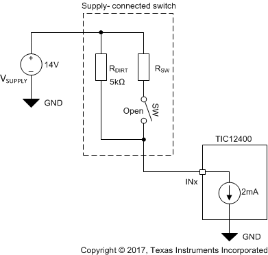 Figure 14. Example showing The Calculation Of The INx Pin Voltage For A Leaky Supply-connected Switch
It is possible to configure an input to ADC input mode, instead of comparator input mode, to monitor single-threshold digital switches. The following programming procedure is recommended under such configuration:
Table 3. Recommended threshold Configuration When Using An ADC Input To Monitor Digital Switches
| Input | Recommended Threshold Configuration |
|---|---|
| IN0 to IN11 | Configure the desired threshold to one of the settings from THRES0 to THRES7 and map it accordingly |
| IN12 to IN17 |
|
| IN18 to IN22 |
|
| IN23 |
|
8.3.8.5 Wetting Current Configuration
There are 6 different wetting current settings (0mA, 1mA, 2mA, 5mA, 10mA, and 15mA) that can be programmed by configuring the WC_CFG0 and WC_CFG1 registers. 0mA is selected by default upon device reset.
To monitor resistor coded switches, a lower wetting current setting (1 mA, 2 mA, or 5 mA) is generally desirable to get the resolution needed to resolve different input voltages while keeping them within the ADC full-scale range (0 V to 6 V). Higher wetting current settings (10mA and 15mA) are useful to clean switch contact oxidation that may form on the surface of an open switch contact. If switch contact cleaning is required for resistor coded switches, the clean current polling (CCP) feature can be activated to generate short cleaning pulses periodically using higher wetting current settings at the end of every polling cycle.
The accuracy of the wetting current has stronger dependency on the VS voltage when VS voltage is low. The lower the VS voltage falls, the more deviation on the wetting currents from their nominal values. Refer to IWETT (CSO) and IWETT (CSI) specifications for more details.
8.3.9 Interrupt Generation and INT Assertion
The INT pin is an active-low, open-drain output that asserts low when an event (switch input state change, temperature warning, over-voltage shutdown…etc) is detected by the TIC12400. An external pull-up resistor to VDD is needed on the INT pin (see Figure 15). If VDD supply is absent, the INT output is functional provided that it is pulled up to a different supply voltage. The INT pin can tolerate up to 40 V but is recommended to be kept below 35V for normal operation.
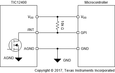 Figure 15. INT Connection Example #1
8.3.9.1 INT Pin Assertion Scheme
TIC12400 supports two configurable schemes for INT assertion: static and dynamic. The scheme can be adjusted by configuring the INT_CONFIG bit in the CONFIG register.
If the static INT assertion scheme is used (INT_CONFIG = 0 in the CONFIG register), the INT pin is asserted low upon occurrence of an event. The INT pin is released on the rising edge of CS only if a READ command has been issued to read the INT_STAT register while CS is low, otherwise the INT will be kept low indefinitely. The content of the INT_STAT interrupt register is latched on the first rising edge of SCLK after CS goes low for every SPI transaction, and the content is cleared upon a READ command issued to the INT_STAT register, as illustrated in Figure 16.
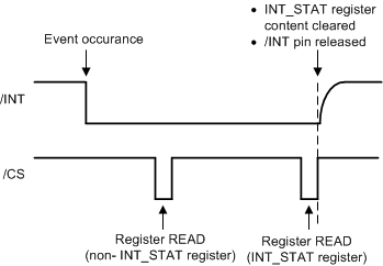 Figure 16. Static INT Assertion Scheme
In some system implementation, an edge-triggered based microcontroller might potentially miss the INT assertion if it is configured to the static scheme, especially when the microcontroller is in the process of waking up. To prevent missed INT assertion and improve robustness of the interrupt behavior, the TIC12400 provides the option to use the dynamic assertion scheme for the INT pin. When the dynamic scheme is used (INT_CONFIG= 1 in the CONFIG register), the INT pin is asserted low for a duration of tINT_ACTIVE, and is de-asserted back to high if the INT_STAT register has not been read after tINT_ACTIVE has elapsed. The INT is kept high for a duration of tINT_INACTIVE, and is re-asserted low after tINT_INACTIVE has elapsed. TheINT pin continues to toggle until the INT_STAT register is read.
If the INT_STAT register is read when INT pin is asserted low, the INT pin is released on the READ command’s CS rising edge and the content of the INT_STAT register is also cleared, as shown in Figure 17. If the INT_STAT register is read when INT pin is de-asserted, the content of the INT_STAT register is cleared on the READ command’s CS rising edge, and the INT pin is not re-asserted back low, as shown in Figure 18.
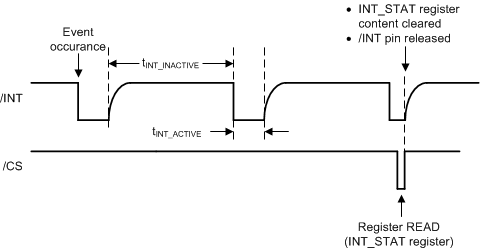 Figure 17. INT Assertion Scheme With INT_STAT Register Read During tINT_ACTIVE
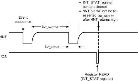 Figure 18. Dynamic INT Assertion Scheme With INT_STAT Register Read During tINT_INACTIVE
The static INT assertion scheme is selected by default upon device reset. The INT pin assertion scheme can only be changed when bit TRIGGER is logic 0 in the CONFIG register.
8.3.9.2 Interrupt Idle Time (tINT_IDLE) Time
Interrupt idle time (tINT_IDLE) is implemented in TIC12400 to:
- Allow the INT pin enough time to be pulled back high by the external pull-up resistor to allow the next assertion to be detectable by an edge-triggered microcontroller.
- Minimize the chance of glitching on the INT pin if back-to-back events occur.
When there is a pending interrupt event and the interrupt event is not masked, tINT_IDLE is applied after the READ command is issued to the INT_STAT register. If another event occurs during the interrupt idle time, the INT_STAT register content is updated instantly, but the INT pin is not asserted low until tINT_IDLE has elapsed. If another READ command is issued to the INT_STAT register during tINT_IDLE, the INT_STAT register content is cleared immediately, but the INT pin is not re-asserted back low after tINT_IDLE has elapsed. An example of the interrupt idle time is given below to illustrate the INT pin behavior under the static /INT assertion schemes:
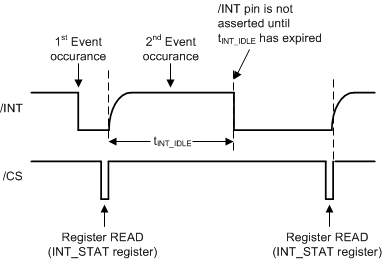 Figure 19. INT Assertion Scheme With tINT_IDLE
8.3.9.3 Microcontroller Wake-Up
When used together with external PNP transistors, the INT pin could also be used for wake-up purpose to activate a voltage regulator via its inhibit inputs (see Figure 20). This is especially useful for waking up a microcontroller in sleep mode. Before the wake-up, the VDD could be unavailable to the TIC12400 and the INT pin can be pulled up externally to the VS voltage. When an event (switch status change, temperature warning, or OV…etc) takes place, the INT pin will be asserted low to activate the voltage regulator, which in turn activates the microcontroller to enable the communication between the microcontroller and the TIC12400. The event information is stored inside the device interrupt register (INT_STAT) for the microcontrollers retrieval when the communication is reestablished.
The wake-up implementation is applicable only when the device is configured to use the static INT assertion scheme.
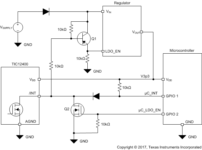 Figure 20. INT Connection to Support Microcontroller Wake-Up
8.3.9.4 Interrupt Enable/disable And Interrupt generation Conditions
Each switch input can be programmed to enable or disable interrupt generation upon status change by configuring registers INT_EN_COMP1 to INT_EN_COMP2 (for comparator inputs) and INT_EN_CFG1 to INT_EN_CFG4 (for ADC inputs). Interrupt generation condition can be adjusted for THRES_COM (for IN0-IN11) by adjusting the IN_COM_EN bit in the MATRIX register.
The abovementioned registers can also be used to control interrupt generation condition based on the following settings:
- Rising edge: an interrupt is generated if the current input measurement is above the corresponding threshold and the previous measurement was below.
- Falling edge: an interrupt is generated if the current input measurement is below the corresponding threshold and the previous measurement was above.
- Both edges: changes of the input voltage in either direction results in an interrupt generation.
Note interrupt generation from switch status change is disabled for all inputs by default upon device reset.
8.3.9.5 Detection Filter
When monitoring the switch input status, an detection filter can be configured by setting the DET_FILTER bits in the CONFIG register to generate switch status change (SSC) interrupt only if the same input status (w.r.t the threshold) is sampled consecutively. This detection filter can be useful to debounce inputs during switch toggle event. Four different filtering schemes are available:
- Generate an SSC interrupt if the voltage level at an input crossed its threshold
- Generate an SSC interrupt if the voltage level at an input crossed its threshold and the status is stable (w.r.t. the threshold) for at least 2 consecutive polling cycles
- Generate an SSC interrupt if the voltage level at an input crossed its threshold and the status is stable (w.r.t. the threshold) for at least 3 consecutive polling cycles
- Generate an SSC interrupt if the voltage level at an input crossed its threshold and the status is stable (w.r.t. the threshold) for at least 4 consecutive polling cycles
The default value of switch status is stored internally after the 1st detection cycle, even if detection filter (by configure the DET_FILTER in the CONFIG register) is used. An example is illustrated below with the assumption that DET_FILTER in register CONFIG is set to 11 (SSC interrupt generated if the input crosses threshold and the status is stable w.r.t. the threshold for at least 4 consecutive detection cycles). Assume switch status change is detected in the 3rd detection cycle and stays the same for the next 3 cycles.
| Detection cycle | 1 | 2 | 3 | 4 | 5 | 6 |
|---|---|---|---|---|---|---|
| Event |
|
— | Switch status change detected | — | — |
|
Tthe detection filter applies to all enabled inputs regardless its input modes (ADC or comparator) selection. The detection filter counter is reset to 0 when the TRIGGER bit in the CONFIG register is de-asserted to logic 0. Upon device reset, the default setting for the detection filter is set to generating an SSC interrupt at every threshold crossing.
Note the detection filter does not apply to the common threshold THRES_COM.
8.3.10 Temperature Monitor
With multiple switch inputs closed and high wetting current setting enabled, considerable power could be dissipated by the device and raise the device temperature. TIC12400 has integrated temperature monitoring and protection circuitry to prevent permanent device damage resulted from device overheating. Two types of temperature protection mechanisms are integrated in the device: Temperature Warning (TW) and Temperature Shutdown (TSD). The triggering temperatures and hysteresis are specified in Table 4 below:
Table 4. Temperature Monitoring Characteristics of TIC12400
| Parameter | Min | Typ | Max | Unit |
|---|---|---|---|---|
| Temperature warning trigger temperature (TTW) | 130 | 140 | 155 | °C |
| Temperature shutdown trigger temperature (TTSD) | 150 | 160 | 175 | °C |
| Temperature hysteresis (THYS) for TTW and TTSD | 15 | °C |
8.3.10.1 Temperature Warning (TW)
When the device temperature goes above the temperature warning trigger temperature (TTW), the TIC12400 performs the following operations:
- Generate an interrupt by asserting the INT pin low and flag the TW bit in INT_STAT register to logic 1. The TEMP bit in the SPI flag is also flagged to logic 1 for all SPI transactions.
- The TW_STAT bit of the IN_STAT_MISC register is flagged to logic 1.
- If the TW_CUR_DIS_CSO or TW_CUR_DIS_CSO bit in CONFIG register set to logic 0 (default), the wetting current is adjusted down to 2 mA for 10 mA or 15 mA settings. The wetting current stays at its pre-configured value if 0 mA, 1 mA, 2 mA, or 5 mA setting is used.
- Maintain the low wetting current as long as the device junction temperature stays above TTW - THYS.
The INT pin is released and the INT_STAT register content is cleared on the rising edge of CS provided the INT_STAT register has been read during CS low. The TIC12400 continues to monitor the temperature, but does not issue further interrupts if the temperature continues to stay above TTW- THYS. The status bit TW_STAT in register IN_STAT_MISC continues to stay at logic 1 as long as the temperature warning condition exists.
If desired, the reduction of wetting current down to 2 mA setting (from 10 mA or 15 mA) can be disabled by setting the TW_CUR_DIS_CSO or TW_CUR_DIS_CSI bit in the CONFIG register to 1. The interrupt is still generated (INT asserted low and INT_STAT interrupt register content updated) when the temperature warning event occurs but the wetting current is not reduced. This setting applies to both the polling and continuous mode operation. Note if the feature is enabled, switch detection result might be impacted upon TTW event if the wetting current is reduced to 2mA from 10mA or 15mA.
When the temperature drops below TTW - THYS, the INT pin is asserted low (if released previously) to notify the microcontroller that the temperature warning condition no longer exists. The TW bit of the interrupt register INT_STAT is flagged logic 1. The TW_STAT bit in the IN_STAT_MISC register is de-asserted back to logic 0. The device resumes operation using the current programmed settings (regardless of the INT and CS status).
8.3.10.2 Temperature Shutdown (TSD)
After the device enters TW condition, if the junction temperature continues to rise and goes above the temperature shutdown threshold (TTSD), the TIC12400 enters the Temperature Shutdown (TSD) condition and performs the following operations:
- Opens all the switches connected to the current sources/sinks to prevent any further heating due to excessive current flow.
- Generate an interrupt by asserting the INT pin (if not already asserted) low and flag the bit TSD in the INT_STAT register to logic 1. The TEMP bit in the SPI flag is also flagged to logic 1 for all SPI transactions.
- The TSD_STAT bit of the IN_STAT_MISC register is flagged to logic 1. The TW_STAT bit also stays at logic 1.
- SPI communication stays on, and all register settings say intact without resetting. Previous switch status, if needed, can be retrieved without any interruption.
- Maintain the setting as long as the junction temperature stays above TTSD - THYS.
The INT pin is released and the INT_STAT register content is cleared on the rising edge of CS provided the INT_STAT register has been read during CS low. The TIC12400 continues to monitor the temperature, but does not issue further interrupts if the temperature continues to stay above TTSD- THYS. The status bit TSD_STAT in register IN_STAT_MISC continues to stay at logic 1 as long as the temperature shutdown condition exists.
When the temperature drops below TTSD - THYS, the INT pin is asserted low (if released previously) to notify the microcontroller that the temperature shutdown condition no longer exists. The TSD bit of the interrupt register INT_STAT is flagged logic 1. In the IN_STAT_MISC register, the TSD_STAT bit is de-asserted back to logic 0, while the TW_STAT bit stays at logic 1. The device resumes operation using the wetting current setting described in section Temperature Warning if the temperature stays above TTW - THYS. Note the polling restarts from the first enabled channel and the SSC interrupt is generated at the end of the first polling cycle. The detected switch status from the first polling cycle becomes the default switch status for subsequent polling.
8.3.11 Parity Check And Parity Generation
The TIC12400 uses parity bit check to ensure error-free data transmission from/to the SPI master.
The device uses odd parity, for which the parity bit is set so that the total number of ones in the transmitted data on SO (including the parity bit) is an odd number (that is, Bit0 ⊕ Bit1 ⊕ ….⊕ Bit30 ⊕ Bit31⊕ Parity = 1).
The device also does odd parity check after receiving data on SI from the SPI master. If the total number of ones in the received data (including the parity bit) is an even number, the received data is discarded. The INT will be asserted low and the PRTY_FAIL bit in the interrupt register (INT_STAT) is flagged to logic 1 to notify the host that transmission error occurred. The PRTY_FAIL flag is also asserted during SPI communications.
8.3.12 Cyclic Redundancy Check (CRC)
The TIC12400 includes a CRC module to support redundancy checks on the configuration registers to ensure the integrity of data. The CRC calculation is based on the ITU-T X.25 implementation, and the CRC polynomial (0x1021) used is popularly known as CRC-CCITT-16 since it was initially proposed by the ITU-T (formerly CCITT) committee. The CRC calculation rule is defined as:
Table 5. CRC calculation rule
| CRC Rule | Value |
|---|---|
| CRC result width | 16 bits |
| Polynomial | x^16+ x^12+ x^5+1 (1021h) |
| Initial (seed) value | FFFFh |
| Input data reflected | No |
| Result data reflected | No |
| XOR value | 0000h |
The CRC calculation is done on all the configuration registers starting from register CONFIG and ending at register MODE. The device substitutes a “zero” for each reserved configuration register bit during the CRC calculation. The CRC calculation can be triggered by asserting the CRC_T bit in the CONFIG register. Once completed, the CRC_CALC interrupt bit in the INT_STAT register is asserted and an interrupt is issued, The 16-bit CRC calculation result is stored in the register CRC. This interrupt can be disabled by de-asserting the CRC_CALC_EN bit in the INT_EN_CFG0 register. It is important to avoid writing data to the configuration registers when the device is undergoing CRC calculations to prevent generation of any false calculation result.
The diagram below shows the block diagram of the CRC module. The module consists of 16 shift-registers and 3 exclusive-OR gates. The registers start with 1111-1111-1111-1111 (or FFFFh) and the module performs XOR action and shifts its content until the last bit of the register string is used. The final register’s content after the last data bit is the calculated CRC value of the data set and the content is stored in the CRC register.
Note the CRC_T bit is self-clearing after CRC calculation is completed. Logic 1 is used for CRC_T bit during CRC calculation.
 Figure 21. CCITT-16 CRC Module Block Diagram
8.4 Device Functional Modes
The TIC12400 has 2 modes of operation: continuous mode, and polling mode. The following sections describe the two operation modes in details, as well as some of the advanced features that could be activated during normal operations.
8.4.1 Continuous Mode
In continuous mode, wetting current is continuously applied to each enabled input channel, and the status of each channel is sampled sequentially (starting from the IN0 to IN23). The TIC12400 monitors enabled inputs and issues an interrupt (if enabled) if switch status change event is detected. The wetting current setting for each input can be individually adjusted by configuring the WC_CFG0 and WC_CFG1 to the 0 mA, 1 mA, 2 mA, 5 mA, 10 mA, or 15 mA setting. Each input is monitored by either a comparator or an ADC depending on the setting of the input mode in the register MODE.
Figure 22 below illustrates an example of the timing diagram of the detection sequence in continuous mode. After the TRIGGER bit in register CONFIG is set to logic 1, it takes tSTARTUP to activate the wetting current for all enabled inputs. The wetting currents stay on continuously, while each input is routed to the ADC/comparator for sampling in a sequential fashion. After conversion/comparison is done for an input, the switch status (below or above detection threshold) is stored in registers (IN_STAT_COMP for comparator inputs and IN_STAT_ADC0 to IN_STAT_ADC1 for ADC inputs) to be used as the default state for subsequent detection cycles. The digital values (if the input is configured as ADC input mode) are stored inside the registers ANA_STAT0 toANA_STAT11. After the end of the first polling cycle, the INT pin is asserted low to notify the microcontroller that the default switch status is ready to be read. The SSC bit in INT_STAT register and the SPI status flag SSC are also asserted to logic 1. The polling cycle time (tPOLL) determines how frequently each input is sampled and can be configured in the register CONFIG.
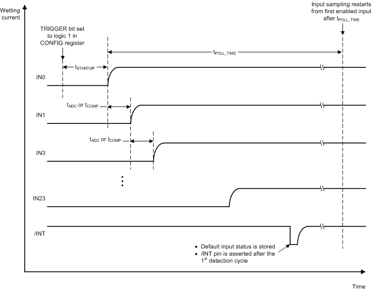 Figure 22. An Example Of The Detection Sequence In continuous Mode
The INT_STAT register is cleared and INT pin de-asserted if a SPI READ commanded is issued to the register. Note the interrupt is always generated after the 1st detection cycle (after the TRIGGER bit in register CONFIG is set to logic 1). In subsequent detection cycles, the interrupt is generated only if switch status change is detected.
No wetting current is applied to the inputs configured to the 0mA setting, although some biasing current (as specified by IIN_LEAK_0mA) may still flow in and out of the input. Threshold crossing monitoring is still performed for the input using the defined threshold(s). The 0mA setting is useful to utilize the integrated ADC or comparator to measure applied voltage on a specific input without getting affected by the device wetting current.
8.4.2 Polling Mode
The polling mode can be activated to reduce current drawn to reduce heat dissipation. Unlike in the continuous mode, the current sources/sinks do not stay on continuously in the polling mode. Instead, they are turned on/off sequentially from IN0 to IN23 and cycled through each individual input channel. The microcontroller can be put to sleep to reduce overall system power. If a switch status change (SSC) is detected by the TIC12400, the INT pin (if enabled for the input channel) is asserted low (and the SSC bit in INT_STAT register and the SPI status flag SSC are also asserted to logic 1). The INT assertion can be used to wake up the system regulator, which in turn wakes up the microcontroller as described in section Microcontroller Wake-Up. The microcontroller can then use SPI communication to read the switch status information.
The polling is activated when the TRIGGER bit in the CONFIG register is set to logic 1. There are 2 different polling schemes that can be configured in TIC12400: standard polling and matrix polling.
8.4.2.1 Standard Polling
In standard polling mode, wetting current is applied to each input for a pre-programmed polling active time set by the POLL_ACT_TIME bits in the CONFIG register between 64us and 2048 us. At the end of the wetting current application, the input voltage is sampled by the comparator (if input is configured as comparator input mode) or the ADC (if input is configured as ADC input mode). Each input is cycled through in sequential order from IN0 to IN23. Sampling is repeated at a frequency set by the POLL_TIME bits in the CONFIG register from 2ms to 4096ms. Wetting currents are applied to closed switches only during the polling active time; hence the overall system current consumption can be greatly reduced.
Similar to continuous mode, after the first polling cycle, the switch status of each input (below or above detection threshold) is stored internally in registers (IN_STAT_COMP for comparator inputs and IN_STAT_ADC0 to IN_STAT_ADC1 for ADC inputs) to be used as the default state for subsequent polling cycles. The digital values (if the input is configured as ADC input mode) are stored inside the registers ANA_STAT0 toANA_STAT11. The INT pin is asserted low to notify the microcontroller that the default switch status is ready to be read. The SSC bit in INT_STAT register and the SPI status flag SSC are also asserted to logic 1. The INT_STAT register is cleared and /INT pin de-asserted if a SPI READ commanded is issued to the register. Note the interrupt is always generated after the 1st polling cycle (after the TRIGGER bit in register CONFIG is set to logic 1). In subsequent polling cycles, the interrupt is generated only if switch status change is detected.
An example of the timing diagram of the polling mode operation is shown in Figure 23. Note in this example, IN1 is set to comparator input mode, while the other inputs are set to ADC input mode. As a result, the wetting current applied to IN2 is activated faster (tCOMP instead of tADC after IN1 wetting current turns off) to shorten the overall polling period. Shortened polling period translates to reduced overall power consumption for the system.
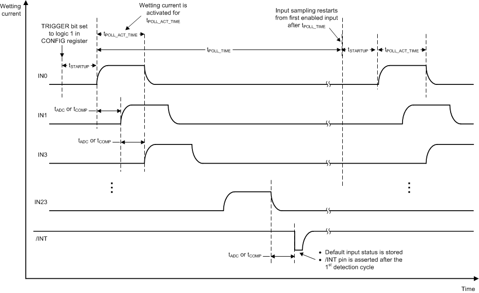 Figure 23. An Example Of The Polling Sequence In Standard Polling Mode
If the switch position changes between two active polling times, no interrupt will be generated and the status registers (IN_STAT_COMP for comparator inputs and IN_STAT_ADC0 to IN_STAT_ADC1 for ADC inputs) will not reflect such a change. An example is shown in Figure 24.
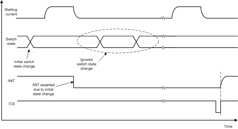 Figure 24. Example For Ignored Switch Position Change Between 2 Wetting Current Cycles
8.4.2.2 Matrix Polling
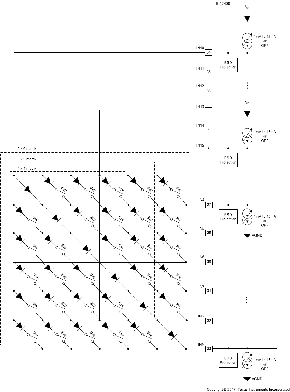 Figure 25. TIC12400 Matrix Configuration
From IN4 to IN15, a special input switch matrix (see Figure 25) can be configured and monitored in addition to the standard switches to GND and VSUPPLY. This feature could be useful to monitor a special switch input configuration call Matrix, as required by some specific OEMs.
Three different matrix configurations are possible, and are defined by MATRIX bits in the MATRIX register. If the MATRIX bits are set to ‘00’, all inputs are treated as standard inputs with identical polling active time according to the POLL_ACT_TIME bits in the CONFIG register. Any settings other than ‘00’ for MATRIX bits causes the polling active time for the matrix inputs to be configured according to POLL_ACT_TIME_M bits in the MATRIX register. Inputs that are not part of the matrix configuration will be configured using the POLL_ACT_TIME bits in the CONFIG register. tPOLL_ACT_TIME_M should be configured properly to allow sufficient time for the current source/sink to charge/discharge the capacitors (if any) connected to the switch inputs.
Table 6. TIC12400 Matrix Configuration Settings
| Input | 4x4 matrix | 5x5 matrix | 6x6 matrix | |||
|---|---|---|---|---|---|---|
| Current Source Or Sink | Polling Active Time Setting | Current Source Or Sink | Polling Active Time Setting | Current Source Or Sink | Polling Active Time Setting | |
| IN4 | CSI | POLL_ACT_TIME_M | CSI | POLL_ACT_TIME_M | CSI | POLL_ACT_TIME_M |
| IN5 | CSI | CSI | CSI | |||
| IN6 | CSI | CSI | CSI | |||
| IN7 | CSI | CSI | CSI | |||
| IN8 | Configurable to CSO or CSI | POLL_ACT_TIME | CSI | CSI | ||
| IN9 | Configurable to CSO or CSI | Configurable to CSO or CSI | POLL_ACT_TIME | CSI | ||
| IN10 | CSO | POLL_ACT_TIME_M | CSO | POLL_ACT_TIME_M | CSO | |
| IN11 | CSO | CSO | CSO | |||
| IN12 | CSO | CSO | CSO | |||
| IN13 | CSO | CSO | CSO | |||
| IN14 | CSO | POLL_ACT_TIME | CSO | CSO | ||
| IN15 | CSO | CSO | POLL_ACT_TIME | CSO | ||
The TIC12400 implements a different polling scheme when matrix input is configured. After the polling sequence is started (by setting TRIGGER bit in CONFIG register to logic 1), the polling takes place within the matrix input group first before the rest of the standard inputs are polled. After the matrix inputs are polled, the switch status of each input combination (below or above detection threshold) is stored internally in registers IN_STAT_MATRIX0 and IN_STAT_MATRIX1, and it is used as the default state for subsequent matrix polling cycles. The standard inputs follow the same polling behavior as described in section Standard Polling. After the polling cycle (matrix+ standard) is completed, the INT pin is asserted low to notify the microcontroller that the default switch status is ready to be read. The SSC bit in the INT_STAT register and the SPI status flag SSC are also asserted to logic 1.
The INT_STAT register is cleared and INT pin de-asserted if a SPI READ commanded is issued to the register. Note the interrupt is always generated after the 1st complete polling cycle (after the TRIGGER bit in register CONFIG is set to logic 1). In subsequent polling cycles, the interrupt is generated only if switch status change is detected.
Note the following programming requirement when using the matrix polling:
- It is critical to program the CSO/CSI configuration for each matrix input appropriately according to Table 6 to avoid incorrect switch status detection.
- It is mandatory to set higher wetting current for the sinks (IN4-IN9) than the sources (IN10-IN15). The actual current flowing through the external switches will be the lesser of the two settings. If the same setting is used for both the sink and the source, the detected result might be incorrect. Because of this, 15mA setting shall not be used for the current sources and 1 mA setting shall not be used for the current sinks. Depending on the type of matrix switches, the TIC12400 might require some specific wetting current settings to be able to distinguish between switch open/closed states.
- If TW_CUR_DIS_CSO or TW_CUR_DIS_CSI is set to logic 0 in the CONFIG register, wetting current is reduced to 2 mA for 10 mA and 15 mA settings upon TW event. Since it’s mandatory to have higher wetting current for the sinks (IN4-IN9) than the sources (IN10-IN15) during matrix polling,Table 7 below summarizes the only possible settings if TW event is expected:
Table 7. Possible Wetting Current Settings For The Matrix Polling Mode If TW_CUR_DIS=0 And TW Event Is Expected
| CSO (IN10-IN15) | CSI (IN4-IN9) | Resulting wetting current |
|---|---|---|
| 1 mA | 2 mA, 5 mA, 10 mA, 15 mA | 1 mA |
| 2 mA | 5 mA | 2 mA |
If higher wetting current is needed and TW event might be expected, the TW wetting current reduction feature needs to be disabled by setting TW_CUR_DIS_CSO or TW_CUR_DIS_CSI bit in the CONFIG register to 1.
- Only comparator input mode is supported for the matrix polling. Do not program the matrix inputs into ADC input mode. The comparison takes place on the source side (IN10-IN15) since the sink side is pulled to ground. Interrupt generation condition can be set by configuring the INT_EN_COMP1and INT_EN_COMP2 registers for inputs IN10 to IN15.
Some programmability is removed when matrix polling mode is used, as listed below:
- To keep the polling scheme simple, the ability to disable inputs is removed for the matrix inputs. Only 3 configurations (4x4, 5x5, and 6x6) can be used for the matrix polling. Standard inputs outside the matrix input group can still be disabled, if desired.
- Detection filter (by configure the DET_FILTER in the CONFIG register) does not apply to the matrix inputs, but still applies to the standard inputs outside the matrix input group.
- When matrix polling is selected, continuous mode is not available to the standard inputs outside the matrix input group.
Figure 26 illustrates an example of the polling sequence for the 6x6 matrix input configuration:
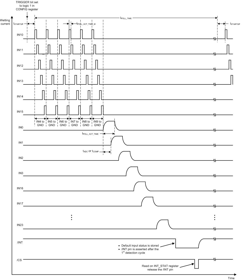 Figure 26. Polling Scheme for 6x6 Matrix Inputs
Figure 27 illustrates an example of the polling sequence for the 5x5 matrix input configuration. Note the input IN9 and IN15 are included in the standard polling sequence.
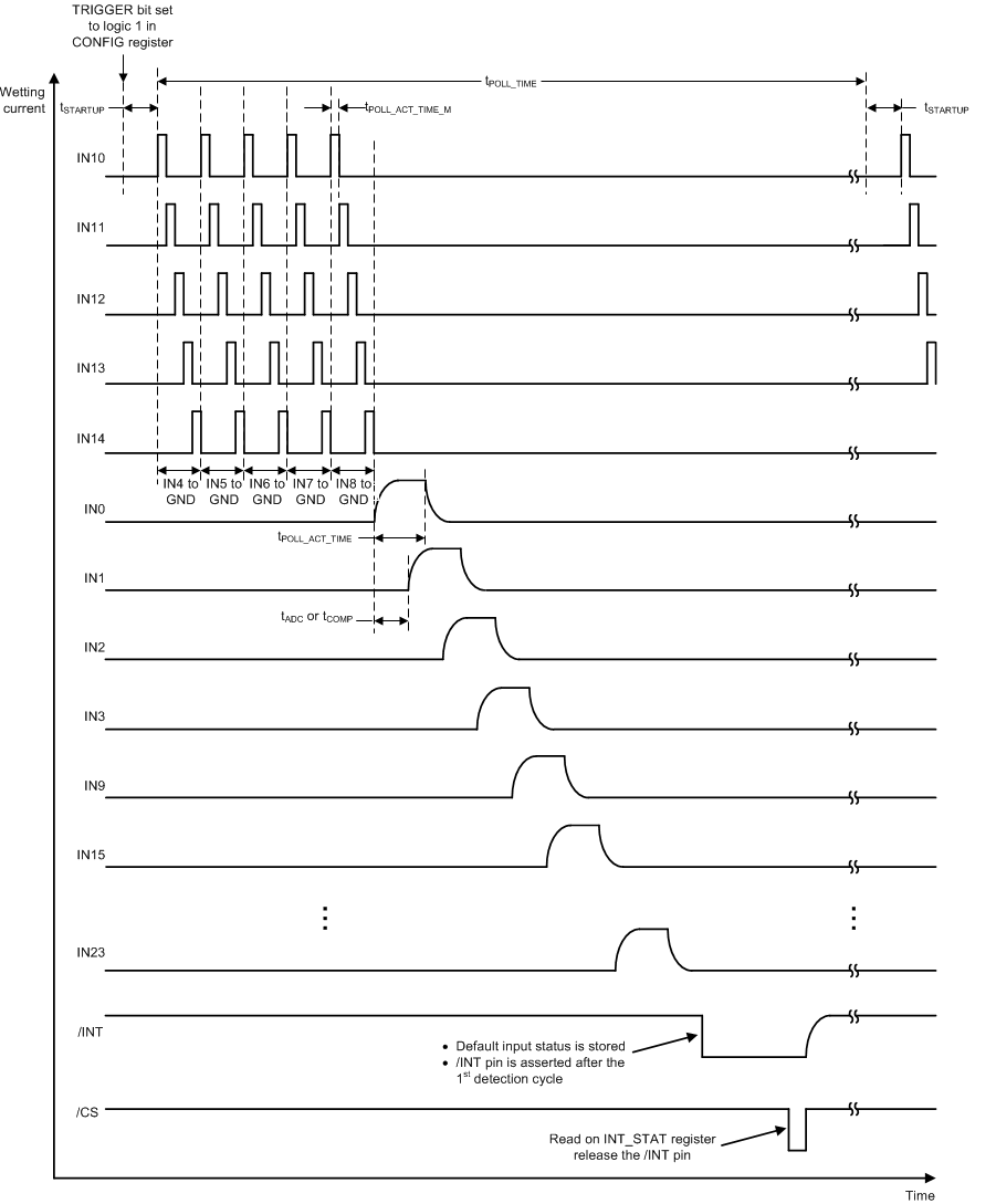 Figure 27. Polling Scheme For 5x5 Matrix Inputs
Figure 28 illustrates an example of the polling sequence for the 4x4 matrix input configuration. Note inputs IN8, IN9, IN14, and IN15 are included in the standard polling sequence.
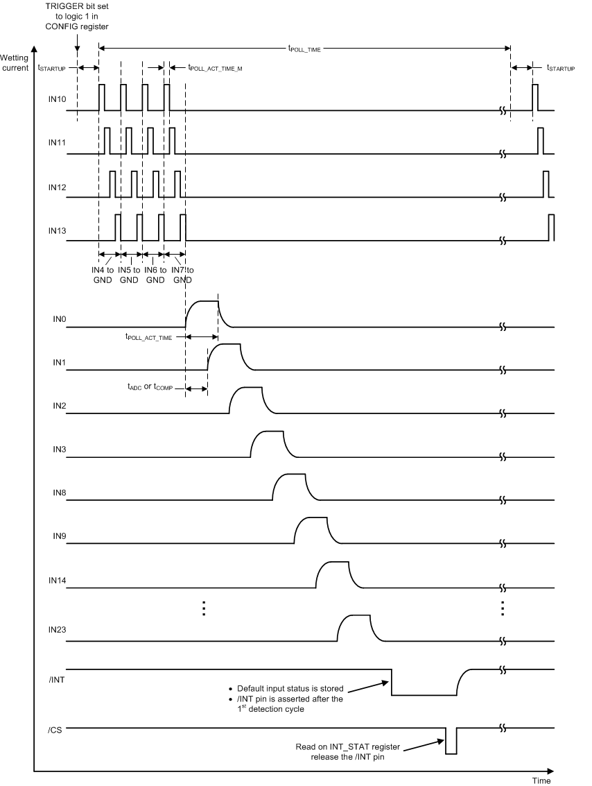 Figure 28. Polling Scheme For 4x4 Matrix Inputs
8.4.3 Additional Features
There are additional features that can be enabled during continuous and polling mode to increase robustness of device operation or provide more system information. These features are described in detail in the following sections:
8.4.3.1 Clean Current Polling (CCP)
To detect resistor coded switches or reduce overall power consumption of the chip, a lower wetting current setting might be desired. However, certain system design requires 10mA or higher cleaning current to clear oxide build-up on the mechanical switch contact surface when the current is applied to closed switches. A special type of polling, called the Clean Current Polling (CCP) can be used for this application.
If CCP is enabled, each polling cycle consists of two wetting current activation steps. The first step uses the wetting current setting configured in the WC_CFG0 and WC_CFG1 registers as in the continuous mode or polling mode. The second step (cleaning cycle) is activated simultaneously for all CCP enabled inputs tCCP_TRAN after the normal polling step of the last enabled input. Interrupt generation and INT pin assertion is not impacted by the clean current pulses.
The wetting current and its active time for the cleaning cycle can be configured in the CCP_CFG0 register. The cleaning cycle can be disabled, if desired, for each individual input by programming the CCP_CFG1 register. CCP is available for both continuous mode and the polling mode. To use the CCP feature, at least one input (standard or matrix) or the VS measurement has to be enabled.
Note that although CCP can be enabled in Matrix polling mode, it is not an effective way to clean the matrix switch contact, since the current supplied from the TIC12400 is divided and distributed across multiple matrix channels.
Figure 29 illustrates the operation of the CCP when the device is configured to the standard polling mode.
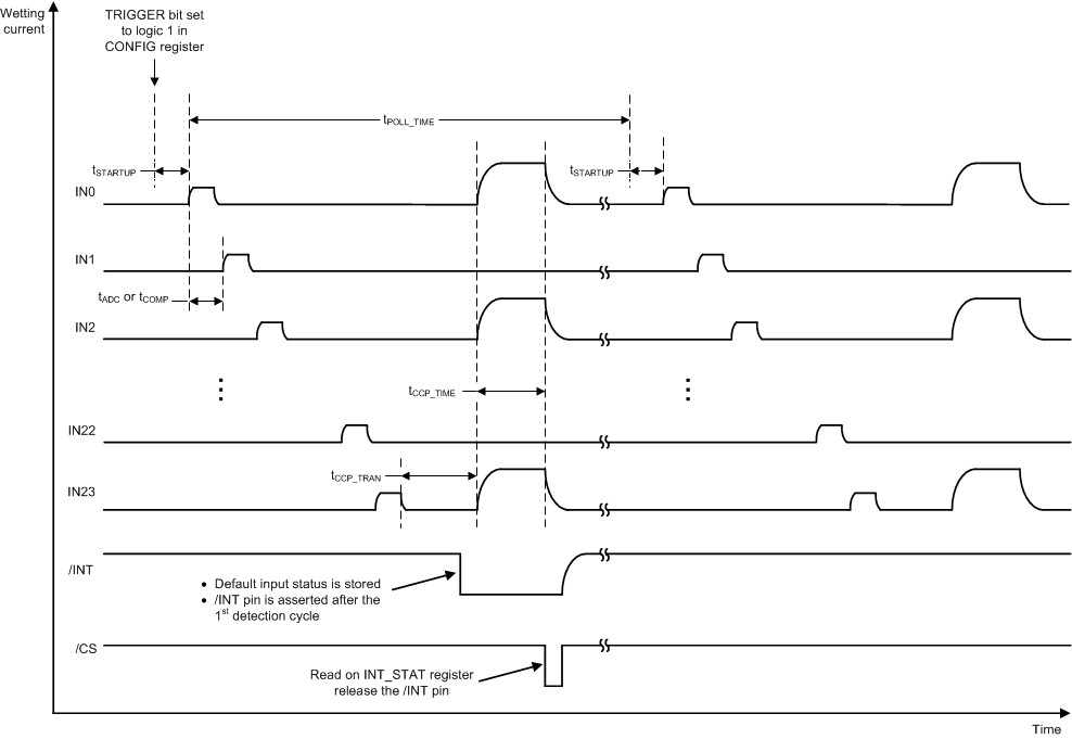 Figure 29. Standard Polling With CCP Enabled
Figure 30 illustrates the operation of the CCP when the device is configured to the continuous mode:
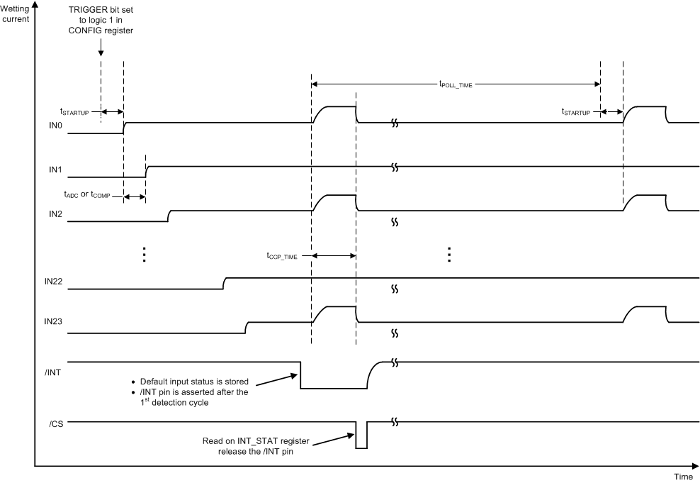 Figure 30. Continue Mode With CCP Enabled
8.4.3.2 Wetting Current Auto-Scaling
The 10 mA and 15 mA wetting current settings are useful to clean oxide build-up on the mechanical switch contact surface when the switch changes state from open to close. After the switch is closed, it might be undesirable to keep the wetting current level at high level if only digital switches are monitored since it results in high current consumption and could potentially heat up the device quickly if multiple inputs are monitored. The wetting current auto-scaling feature help mitigate this issue.
When enabled (AUTO_SCALE_DIS_CSO or AUTO_SCALE_DIS_CSI bit = logic 0 in the WC_CFG1 register), wetting current is reduced to 2 mA from 10 mA or 15 mA setting after switch closure is detected. The threshold used to determine a switch closure is the threshold configured in the THRES_COMP register for inputs configured as comparator input mode. For inputs configured as ADC input mode, the threshold used to determine a switch closure depends on the input number, as described in Table 8 below:
Table 8. Threshold Used To Determine A Switch Closure For Wetting Current Auto-scaling For ADC Inputs
| Input | Threshold used to determine a switch closure |
|---|---|
| IN0-IN11 | Mapped threshold from THRES0 to THRES7 |
| IN12 to IN17 | THRES2B |
| IN18 to IN22 | THRES3C |
| IN23 | THRES9 |
The current reduction takes place N cycles after switch closure is detected on an input, where N depends on the setting of the DET_FILTER bits in the CONFIG register:
- DET_FILTER= 00: wetting current is reduced immediately in the next detection cycle after a closed switch is detected.
- DET_FILTER= 01: wetting current is reduced when a closed switch is detected and the switch status is stable for at least 2 consecutive detection cycles
- DET_FILTER= 10: wetting current is reduced when a closed switch is detected and the switch status is stable for at least 3 consecutive detection cycles
- DET_FILTER= 11: when a closed switch is detected and the switch status is stable for at least 4 consecutive detection cycles
The wetting current is adjusted back to the original setting of 10 mA or 15 mA N cycles after an open switch is detected, where N again depends on the DET_FILTER bit setting in the CONFIG register. Figure 31 depicts the behavior of the wetting current auto-scaling feature.
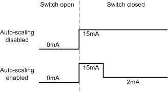 Figure 31. Wetting Current Auto-scaling Behavior
The wetting current auto-scaling only applies to 10 mA and 15 mA settings and is only available in continuous mode. If AUTO_SCALE_DIS_CSO or AUTO_SCALE_DIS_CSI bit is set to logic 1 in the WC_CFG1 registers, the wetting current stays at its original setting when a closed switch is detected. Power dissipation needs to be closely monitored when wetting current auto-scaling is disabled for multiple inputs as the device could heat up quickly when high wetting current settings are used. If the auto-scaling feature is disabled in continuous mode, total power dissipation can be calculated using Equation 1 below.

where IWETT (TOTOAL) is the sum of all wetting currents from all input channels. Increase in device junction temperature can be calculated based on P ×RθJA. The junction temperature has to be limited below TTSD for proper device operation. An interrupt will be issued when the junction temperature exceeds TTW or TTSD. For detailed description of the temperature monitoring, please refer to sections Temperature Warning (TW)and Temperature Shutdown (TSD).
8.4.3.3 VS Measurement
When the TIC12400 is used to monitor resistor-coded switches, the level of VS supply voltage becomes very critical. If VS is not sufficiently high, the device might not have enough headroom to produce accurate wetting currents. This could impact the accuracy of the switch status monitoring. It is imperative for the microcontroller to have knowledge of the VS voltage on a constant basis in such a case.
Measurement of VS voltage is a feature in TIC12400 that can be enabled by setting the VS_MEAS_EN bit in register CONFIG to logic 1. If enabled, at the end of every detection/polling cycle, the voltage on the VS pin is sampled and converted by the ADC to an digital value. The conversion takes one extra tADC, and the converted value is recorded in the ANA_STAT12 register.
The VS measurement supports two different VS voltage ranges that can be configured by the VS_RATIO bit in the CONFIG register. By default (VS_RATIO = logic 0), the supported VS voltage range is from 6.5 V to 9 V, and VS voltage in excess of 9 V results in a saturated ADC raw code of 1023. This setting provides better measurement resolution at lower VS voltages. When VS_RATIO bit is set to logic 1, the supported VS voltage range is widened to 6.5V to 30V, and VS voltage in excess of 30 V results in a saturated ADC raw code of 1023. This setting allows wider measurement range but more coarse measurement resolution. It is important to adjust the detection thresholds accordingly depending on the VS voltage range configured.
Four different thresholds (VS0_THRES2A/B and VS1_THRES2A/B) can be programmed to have the TIC12400 notify the microcontroller when the VS voltage crosses the thresholds. The value of these thresholds can be programmed by configuring registers THRES_CFG0 to THRES_CFG3 and the mapping can be programmed by configuring registers THRESMAP_VS0_THRES2A/B and THRESMAP_VS1_THRES2A/B bits in the register THRESMAP_CFG2. When setting the thresholds, follow the rules in Table 9 below:
Table 9. Proper threshold configuration for VS measurements
| VS Threshold | Proper Threshold Configuration |
|---|---|
| VS0 | VS0_THRES2B ≥ VS0_THRES2A |
| VS1 | VS1_THRES2B ≥ VS1_THRES2A |
After the VS measurement is enabled for the first time, the VS measurement interrupt is always generated (INT pin is asserted low, and the VS0 or VS1 bit in the INT_STAT register is flagged to logic 1) at the end of the first polling cycle to notify the microcontroller the initial VS measurement result is ready to be retrieved . The VS0_STAT and VS1_STAT bits from register IN_STAT_MISC indicate the status of the VS voltage with respect to the thresholds, and the ANA_STAT12 register stores the converted digital value of the VS voltage. The SPI status flag VS_TH is also asserted to logic 1 during SPI communications. Note the status detected in the first polling cycle becomes the baseline value of comparison for subsequent VS measurements and the interrupt will be generated only if threshold crossing is detected.
Similar to regular inputs, interrupt generation condition can be programmed by setting the VS_TH0_EN and VS_TH1_EN bits in the INT_EN_CFG4 register to the following settings:
- Rising edge: an interrupt is generated if the current VS measurement is above the corresponding threshold and the previous measurement was below.
- Falling edge: an interrupt is generated if the current VS measurement is below the corresponding threshold and the previous measurement was above.
- Both edges: changes of the VS measurement status in either direction results in an interrupt generation.
Interrupt generation can also be disabled by setting VS_TH0_EN or VS_TH1_EN to logic 0 in register INT_EN_CFG4. Once disabled, VS voltage crossing does not flag the VS0 or VS1 bit in INT_STAT register and does not assert INT pin low. To only mask the INT pin from assertion (while keeping INT_STAT register updated), configure the VS1_EN and VS0_EN bits in register INT_EN_CFG0 to logic 0.
Note the VS measurement is only intended to be used as part of switch detection sequence to determine the validity of the switch detection states that are reported by the TIC12400. It is not intended to be used for standalone supply monitoring, such as monitoring cranking voltages, due to the potentially delayed response being part of the polling sequence. The VS measurement result is accurate for VS above 6.5V.
By default, the VS voltage measurement is disabled upon device reset.
8.4.3.4 Wetting Current Diagnostic
When the TIC12400 is used to monitor safety-critical switches, it might be valuable for the microcontroller to have knowledge of the wetting current sources/ sinks operating status. This can be achieved by activating the wetting current diagnostic feature provided for inputs IN0 to IN3. IN0 and IN1 can be diagnosed for defective wetting current sources, while IN2 and IN3 can be diagnosed for failed current sinks.
The wetting current diagnostic feature can be activated by setting the WET_D_INx_EN bits in the CONFIG register to 1 for the desired inputs, where x can be 0, 1, 2, or 3. If activated, the TIC12400 checks the status of the wetting current sources/sinks for the configured input periodically as part of the polling sequence. If the wetting current is determined to be flawed, the TIC12400 pulls the INT pin low to notify the host and flag the WET_DIAG bit in the INT_STAT register to logic 1. The OI bit in the SPI flag is also asserted during SPI transactions. The microcontroller can then read bits IN0_D to IN3_D in register IN_STAT_MISC to learn more information on which wetting current source/sink is defective.
The wetting current diagnostic is not performed for inputs that are disabled (IN_EN_x bit = 0 in the IN_EN register) from polling, even if the feature if activated for those inputs. Also, it is critical to configure the current source/sink appropriately (CSO for IN0/IN1 and CSI for IN2/IN3) and program the input to ADC input mode before activating the wetting current diagnostic feature to avoid false interrupt from generation. The wetting current diagnostic feature can be performed regardless of the states of external switches, and it is available in both continuous mode and the polling mode.
Figure 32 shows an example of the feature carried out in a typical polling sequence. In this example, it can be observed that the wetting current is activated for duration of tPOLL_ACT+ tADC for each input diagnosed. After IN3 is diagnosed, normal polling sequence resumes and the wetting current is activated for tPOLL_ACT for the rest of the inputs. The diagnostic is not executed on input IN2 in this example since it is disabled.
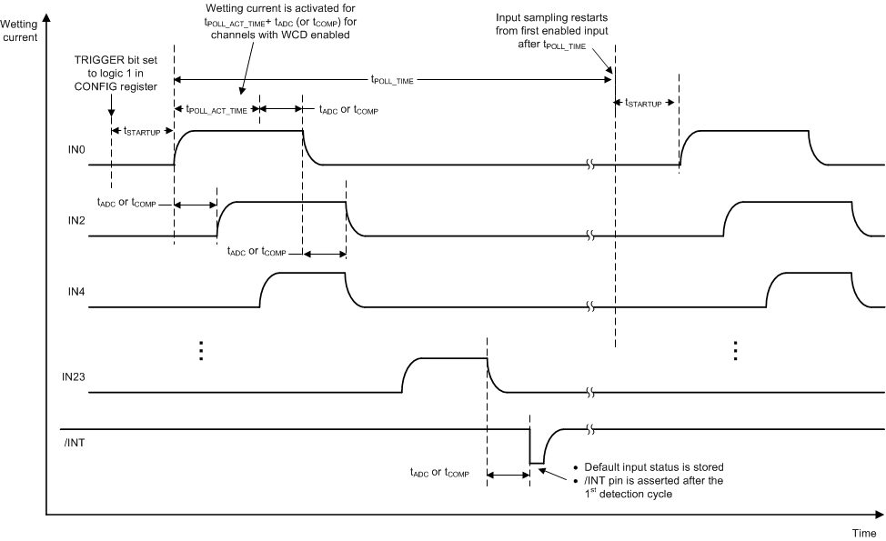 Figure 32. An Example Of The Polling Sequence In Standard Polling Mode With Wetting Current Diagnostic Enabled
8.4.3.5 ADC Self-Diagnostic
In addition to the wetting current diagnostic, another diagnostic feature, the ADC self-diagnostic, can be enabled to monitor the integrity of the internal ADC.
The ADC self-diagnostic feature is activated by setting the ADC_DIAG_T bit in the CONFIG register to logic 1. Once enabled, the TIC12400 periodically sends a test voltage to the ADC. The conversion result is stored in the ADC_SELF_ANA bits in the register ANA_STAT12 and it is compared with a pre-defined code to determine whether the conversion is performed properly. If an error is detected, the TIC12400 pulls the INT pin low to notify the host and flag the ADC_DIAG bit in the INT_STAT to logic 1. The bit ADC_D in register IN_STAT_MISC is updated with the result from the self-diagnostic. The ADC self-diagnostic feature is available in both continuous mode and the polling mode.
8.5 Programming
The SPI interface communication consists of the 4 pins: CS, SCLK, SI, and SO. The interface can work with SCLK frequency up to 4MHz.
8.5.1 SPI Communication Interface Buses
8.5.1.1 Chip Select (CS)
The system microcontroller selects the TIC12400 to receive communication using the CS pin. With the CS pin in a logic LOW state, command words may be sent to the TIC12400 via the serial input (SI) pin, and the device information can be retrieved by the microcontroller via the serial output (SO) pin. The falling edge of the CS enables the SO output and latches the content of the interrupt register INT_STAT. The microcontroller may issue a READ command to retrieve information stored in the registers. Rising edge on the CS pin initiates the following operations:
- Disable the output driver and makes SO high-impedance
- INT pin is reset to logic HIGH if a READ command to the INT_STAT register was issued during CS = LOW.
To avoid any corrupted data, it is essential the HIGH-to-LOW and LOW-to-HIGH transitions of the CS signal occur only when SCLK is in a logic LOW state. A clean CS signal is needed to ensure no incomplete SPI words are sent to the device. The CS pin should be externally pulled up to VDD by a 10-kΩ resistor.
8.5.1.2 System Clock (SCLK)
The system clock (SCLK) pin clocks the internal shift register of the TIC12400. The SI data is latched into the input shift register on the falling edge of the SCLK signal. The SO pin shifts the device stored information out on the rising edge of SCLK. The SO data is available for the microcontroller to read on the falling edge of SCLK.
False clocking of the shift register must be avoided to ensure validity of data and it is essential the SCLK pin be in a logic LOW state whenever CS makes any transition. Therefore, it is recommended that the SCLK pin gets pulled to a logic LOW state as long as the device is not accessed and CS is in a logic HIGH state. When the CS is in a logic HIGH state, any signal on the SCLK and SI pins will be ignored and the SO pin remains as a high impedance output. Refer to Figure 33 and Figure 34 for examples of typical SPI read and write sequence.
8.5.1.3 Slave In (SI)
The SI pin is used for serial instruction data input. SI information is latched into the input register on the falling edge of the SCLK. To program a complete word, 32 bits of information must be enter into the device. The SPI logic counts the number of bits clocked into the IC and enables data latching only if exactly 32 bits have been clocked in. In case the word length exceeds or does not meet the required length, the SPI_FAIL bit of the INT_STAT register is asserted to logic 1 and the INT pin will be asserted low. The data received is considered invalid. Note the SPI_FAIL bit is not flagged if SCLK is not present.
8.5.1.4 Slave Out (SO)
The SO pin is the output from the internal shift register. The SO pin remains high-impedance until the CS pin transitions to a logic LOW state. The negative transition of CS enables the SO output driver and drive the SO output to the HIGH state (by default). The first positive transition of SCLK makes the status data bit 32 available on the SO pin. Each successive positive clock makes the next status data bit available for the microcontroller to read on the falling edge of SCLK. The SI/SO shifting of the data follows a first-in, first-out scheme, with both input and output words transferring the most significant bit (MSB) first.
8.5.2 SPI Sequence
The following diagrams depict the SPI communication sequence during read and write operations for
TIC12400.
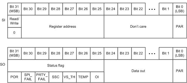 Figure 33. TIC12400 Read SPI Sequence
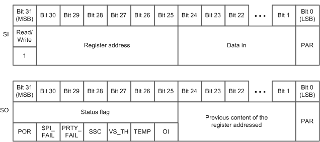 Figure 34. TIC12400 Write SPI Sequence
8.5.2.1 Read Operation
The Read/Write bit (bit 31) of the SI bus needs to be set to logic 0 for a READ operation. The 6-bits address of the register to be accessed follows next on the SI bus. The content from bit 24 to bit 1 does not represent valid command for a read operation and will be ignored. The LSB (bit 0) is the parity bit used to detect communication errors.
On the SO bus, the status flags will be outputted from the TIC12400, followed by the data content in the register that was requested. The LSB is the parity bit used to detect communication errors.
Note there are several test mode registers (not shown in this ASD) used in the TIC12400 in addition to the normal functional registers, and a READ command to these test registers returns the register content. If a READ command is issued to an invalid register address, the TIC12400 will return all 0’s.
8.5.2.2 Write Operation
The Read/Write bit (bit 31) on the SI bus needs to be set to 1 for a write operation. The 6-bits address of the register to be accessed follows next on the SI bus. Note the register needs to be a writable configuration register, or otherwise, the command will be ignored. The content from bit 24 to bit 1 represents the data to be written to the register. The LSB (bit 0) is the parity bit used to detect communication errors.
On the SO bus, the status flags will be outputted from the TIC12400, followed by the previous data content of the same register being written to. The previous data content of the register is latched after the full register address is decoded in the SI command (after bit 25 is transmitted). The new data will replace the previous data content at the end of the SPI transaction if the SI write is a valid command (valid register address and no SPI/parity error). If the write command is invalid, the new data will be ignored and the previous data content of the register stays. The LSB is the parity bit used to detect communication errors.
Note there are several test mode registers (not shown in this ASD) used in the TIC12400 in addition to the normal functional registers. A WRITE command to these test registers have no effect on the register content, though the register content is returned on the SO output. If a WRITE command is issued to an invalid register address, the SO output would returns all 0’s.
8.5.2.3 Status Flag
The status flags are output from SO during every READ or WRITE SPI transaction to indicate system conditions. These bits do not belong to an actual register, but the content is mirrored from the interrupt register INT_STAT. A READ command executed on the INT_STAT would clear both the bits inside the register and the status flag. The following table describes the information that can be obtained from each SPI status flag:
Table 10. TIC12400 SPI Status Flag Description
| Symbol | Name | Description |
|---|---|---|
| POR | Power-on Reset | This flag mirrors the POR bit in the interrupt register INT_STAT and it indicates, if set to 1, that a reset event has occurred. This bit is asserted after a successful power-on=reset, hardware reset or software reset. Refer to section Device Reset for more details. |
| SPI_FAIL | SPI Error | This flag mirrors the SPI_FAIL bit in the interrupt register INT_STAT and it indicates, if set to 1, that the last SPI Slave In (SI) transaction is invalid. To program a complete word, 32 bits of information must be entered into the device. The SPI logic counts the number of bits clocked into the IC and enables data latching only if exactly 32 bits have been clocked in. In case the word length exceeds or does not meet the required size, the SPI_FAIL bit, which mirrors its value to this SPI_FAIL status flag, of the interrupt register INT_STAT will be set to 1 and the INT pin will be asserted low. The data received will be considered invalid. Once the INT_STAT register is read, its content will be cleared on the rising edge of CS. The SPI_FAIL status flag, which mirrors the SPI_FAIL bit in the INT_STAT register, will also be de-asserted. Note the SPI_FAIL bit is not flagged if SCLK is not present. |
| PRTY_FAIL | Parity Fail | This flag mirrors the PRTY_FAIL bit in the interrupt register INT_STAT and it indicates, if set to 1, that the last SPI Slave In (SI) transaction has a parity error. The device uses odd parity. If the total number of ones in the received data (including the parity bit) is an even number, the received data is discarded. The INT will be asserted low and the PRTY_FAIL bit in the interrupt register (INT_STAT) is flagged to logic 1, and the PRTY_FAIL status flag, which mirrors the PRTY_FAIL bit in the INT_STAT register, is also set to 1. Once the INT_STAT register is read, its content will be cleared on the rising edge of CS. The PRTY_FAIL status flag, which mirrors the PRTY_FAIL bit in the INT_STAT register, will also be de-asserted. |
| SSC | Switch State Change | This flag mirrors the SSC bit in the interrupt register INT_STAT and it indicates, if set to 1, that one or more switch input crossed threshold(s). To determine the origin of the state change, the microcontroller can read the content of registers IN_STAT_COMP (if input is set to comparator input mode), IN_STAT_ADC0 to IN_STAT_ADC1 (if input is set to ADC input mode), or IN_STAT_MATRIX0 to IN_STAT_MATRIX1 (if input is set to matrix input). Once the interrupt register (INT_STAT) is read, its content will be cleared on the rising edge of CS. The SSC status flag, which mirrors the SSC bit in the INT_STAT register, will also be de-asserted. |
| VS_TH | VS Threshold Crossing | This flag is set to 1 if either VS0 or VS1 bit in the interrupt register INT_STAT is flagged to 1. It indicates the VS voltage crosses thresholds defined by VS0_THRES2A, VS0_THRES2B, VS1_THRES2A, or VS1_THRES2A. To determine the origin of the threshold crossing, the microcontroller can read register bits VS0_STAT and VS1_STAT in the register IN_STAT_MISC. Once the interrupt register (INT_STAT) is read, its content will be cleared on the rising edge of CS, and the VS_TH status flag will also be de-asserted. |
| TEMP | Temperature event | This flag is set to 1 if either TW or TSD bit in the interrupt register INT_STAT is flagged to 1. It indicates a Temperature Warning (TW) event or a Temperature Shutdown (TSD) event has occurred. It is also flagged to 1 if a Temperature Warning (TW) event or a Temperature Shutdown (TSD) event cleared. The interrupt register INT_STAT should be read to determine which event occurred. The SPI master can also read the IN_STAT_MISC register to get information on the temperature status of the device. Once the interrupt register (INT_STAT) is read, its content will be cleared on the rising edge of CS, and the TEMP status flag will also be de-asserted. |
| OI | Other Interrupt | Other interrupt include interrupts such as OV, UV, CRC_CALC. WET_DIAG, ADC_DIAG and CHK_FAIL. This flag will be asserted 1 when any of the abovementioned bits is flagged in the interrupt register INT_STAT. The interrupt register INT_STAT should be read to determine which event(s) occurred. The SPI master can also read the IN_STAT_MISC register to get information on the latest status of the device. Once the INT_STAT register is read, its content will be cleared on the rising edge of CS, and the OI status flag will also be de-asserted. |
8.6 Register Maps
Table 11 lists the memory-mapped registers for the TIC12400. All register offset addresses not listed in Table 11 should be considered as reserved locations and the register contents should not be modified.
Table 11. TIC12400 Registers
| Offset | Type | Reset | Acronym | Register Name | Section |
|---|---|---|---|---|---|
| 1h | R | 20h | DEVICE_ID | Device ID Register | Go |
| 2h | RC | 1h | INT_STAT | Interrupt Status Register | Go |
| 3h | R | FFFFh | CRC | CRC Result Register | Go |
| 4h | R | 0h | IN_STAT_MISC | Miscellaneous Status Register | Go |
| 5h | R | 0h | IN_STAT_COMP | Comparator Status Register | Go |
| 6h-7h | R | 0h | IN_STAT_ADC0, IN_STAT_ADC1 | ADC Status Register | Go |
| 8h-9h | R | 0h | IN_STAT_MATRIX0, IN_STAT_MATRIX1 | Matrix Status Register | Go |
| Ah-16h | R | 0h | ANA_STAT0- ANA_STAT12 | ADC Raw Code Register | Go |
| 17h-19h | — | — | RESERVED | RESERVED | — |
| 1Ah | R/W | 0h | CONFIG | Device Global Configuration Register | Go |
| 1Bh | R/W | 0h | IN_EN | Input Enable Register | Go |
| 1Ch | R/W | 0h | CS_SELECT | Current Source/Sink Selection Register | Go |
| 1Dh-1Eh | R/W | 0h | WC_CFG0, WC_CFG1 | Wetting Current Configuration Register | Go |
| 1Fh-20h | R/W | 0h | CCP_CFG0, CCP_CFG1 | Clean Current Polling Register | Go |
| 21h | R/W | 0h | THRES_COMP | Comparator Threshold Control Register | Go |
| 22h-23h | R/W | 0h | INT_EN_COMP1, INT_EN_COMP2 | Comparator Input Interrupt Generation Control Register | Go |
| 24h | R/W | 0h | INT_EN_CFG0 | Global Interrupt Generation Control Register | Go |
| 25h-28h | R/W | 0h | INT_EN_CFG1- INT_EN_CFG4 | ADC Input Interrupt Generation Control Register | Go |
| 29h-2Dh | R/W | 0h | THRES_CFG0- THRES_CFG4 | ADC Threshold Control Register | Go |
| 2Eh- 30h | R/W | 0h | THRESMAP_CFG0- THRESMAP_CFG2 | ADC Threshold Mapping Register | Go |
| 31h | R/W | 0h | Matrix | Matrix Setting Register | Go |
| 32h | R/W | 0h | Mode | Mode Setting Register | Go |
8.6.1 DEVICE_ID register (Offset = 1h) [reset = 20h]
DEVICE_ID is shown in Figure 35 and described in Table 12.
Return to Summary Table.
This register represents the device ID of the TIC12400.
| 23 | 22 | 21 | 20 | 19 | 18 | 17 | 16 | 15 | 14 | 13 | 12 |
| RESERVED | |||||||||||
| R-0h | |||||||||||
| 11 | 10 | 9 | 8 | 7 | 6 | 5 | 4 | 3 | 2 | 1 | 0 |
| RESERVED | MAJOR | MINOR | |||||||||
| R-0h | R-2h | R-0h | |||||||||
| LEGEND: R = Read only |
Table 12. DEVICE_ID Register Field Descriptions
8.6.2 INT_STAT Register (Offset = 2h) [reset = 1h]
INT_STAT is shown in Figure 36 and described in Table 13.
Return to Summary Table.
This register records the information of the event as it occurs in the device. A READ command executed on this register clears its content and resets the register to its default value. The INT pin is released at the rising edge of the CS pin from the READ command.
| 23 | 22 | 21 | 20 | 19 | 18 | 17 | 16 |
| RESERVED | |||||||
| R-0h | |||||||
| 15 | 14 | 13 | 12 | 11 | 10 | 9 | 8 |
| RESERVED | CHK_FAIL | ADC_DIAG | WET_DIAG | VS1 | VS0 | CRC_CALC | |
| R-0h | RC-0h | RC-0h | RC-0h | RC-0h | RC-0h | RC-0h | |
| 7 | 6 | 5 | 4 | 3 | 2 | 1 | 0 |
| UV | OV | TW | TSD | SSC | PRTY_FAIL | SPI_FAIL | POR |
| RC-0h | RC-0h | RC-0h | RC-0h | RC-0h | RC-0h | RC-0h | RC-1h |
| LEGEND: R = Read only; RC = Read to clear |
Table 13. INT_STAT Register Field Descriptions
| Bit | Field | Type | Reset | Description |
|---|---|---|---|---|
| 23-14 | RESERVED | R | 0h |
RESERVED |
| 13 | CHK_FAIL | RC | 0h |
0h = Default factory setting is successfully loaded upon device initialization or the event status got cleared after a READ command was executed on the INT_STAT register. 1h = An error is detected when loading factory settings into the device upon device initialization. During device initialization, factory settings are programmed into the device to allow proper device operation. The device performs a self-check after the device is programmed to diagnose whether correct settings are loaded. If the self-check returns an error, the CHK_FAIL bit is flagged to logic 1 along with the POR bit. The host controller is then recommended to initiate a software reset (see section Software Reset) to re-initialize the device and allow correct settings to be re-programmed. |
| 12 | ADC_DIAG | RC | 0h |
0h = No ADC self-diagnostic error is detected or the event status got cleared after a READ command was executed on the INT_STAT register. 1h = ADC self-diagnostic error is detected. The ADC Self-Diagnostic feature (see section ADC Self-Diagnostic) can be activated to monitor the integrity of the internal ADC. The ADC_DIAG bit is flagged to logic 1 if an ADC error is diagnosed. |
| 11 | WET_DIAG | RC | 0h |
0h = No wetting current error is detected, or the event status got cleared after a READ command was executed on the INT_STAT register. 1h = Wetting current error is detected. The Wetting Current Diagnostic feature (see section Wetting Current Diagnostic) can be activated to monitor the integrity of the internal current sources or sinks. The WET_DIAG bit is flagged to logic 1 if an wetting current error is diagnosed. |
| 10 | VS1 | RC | 0h |
0h = No VS voltage state change occurred with respect to VS1_THRES2A or VS1_THRES2B or the status got cleared after a READ command was executed on the INT_STAT register. 1h = VS voltage state change occurred with respect to VS1_THRES2A or VS1_THRES2B. The VS1 interrupt bit indicates whether VS voltage state change occurred with respect to thresholds VS1_THRES2A and VS1_THRES2B if the VS Measurement feature (see section VS Measurement) is activated. |
| 9 | VS0 | RC | 0h |
0h = No VS voltage state change occurred with respect to VS0_THRES2A or VS0_THRES2B or the status got cleared after a READ command was executed on the INT_STAT register. 1h = VS voltage state change occurred with respect to VS0_THRES2A 10or VS0_THRES2B. The VS0 interrupt bit indicates whether VS voltage state change occurred with respect to thresholds VS0_THRES2A and VS0_THRES2B if the VS Measurement feature (see section VS Measurement) is activated. |
| 8 | CRC_CALC | RC | 0h |
0h = CRC calculation is running, not started, or was acknowledged after a READ command was executed on the INT_STAT register. 1h = CRC calculation is finished. CRC calculation (see section Cyclic Redundancy Check (CRC)) can be triggered to make sure correct register values are programmed into the device. Once the calculation is completed, the CRC_CALC bit is flagged to logic 1 to indicate completion of the calculation, and the result can then be accessed from the CRC (offset = 3h) register. |
| 7 | UV | RC | 0h |
0h = No under-voltage condition occurred or cleared on the VS pin, or the event status got cleared after a READ command was executed on the INT_STAT register. 1h = Under-voltage condition occurred or cleared on the VS pin. When the UV bit is flagged to logic 1, it indicates the Under-Voltage (UV) event has occurred. The bit is also flagged to logic 1 when the event clears. For more details about the UV operation, please refer to section VS under-voltage (UV) condition. |
| 6 | OV | RC | 0h |
0h = No over-voltage condition occurred or cleared on the VS pin, or the event status got cleared after a READ command was executed on the INT_STAT register. 1h = Over-voltage condition occurred or cleared on the VS pin. When the OV bit is flagged to logic 1, it indicates the Over-Voltage (OV) event has occurred. The bit is also flagged to logic 1 when the event clears. For more details about the OV operation, please refer to section VS over-voltage (OV) condition. |
| 5 | TW | RC | 0h |
0h = No temperature warning event occurred or the event status got cleared after a READ command was executed on the INT_STAT register. 1h = Temperature warning event occurred or cleared. When the TW bit is flagged to logic 1, it indicates the temperature warning event has occurred. The bit is also flagged to logic 1 when the event clears. For more details about the temperature warning operation, please refer to section Temperature Warning (TW) |
| 4 | TSD | RC | 0h |
0h = No temperature shutdown event occurred or the event status got cleared after a READ command was executed on the INT_STAT register. 1h = Temperature shutdown event occurred or cleared. When the TSD bit is flagged to logic 1, it indicates the temperature shutdown event has occurred. The bit is also flagged to logic 1 when the event clears. For more details about the temperature shutdown operation, please refer to section Temperature shutdown (TSD) |
| 3 | SSC | RC | 0h |
0h = No switch state change occurred or the status got cleared after a READ command was executed on the INT_STAT register. 1h = Switch state change occurred. The Switch State Change (SSC) bit indicates whether input threshold crossing has occurred from switch inputs IN0 to IN23. This bit is also flagged to logic 1 after the first polling cycle is completed after device polling is triggered. |
| 2 | PRTY_FAIL | RC | 0h |
0h = No parity error occurred in the last received SI stream or the error status got cleared after a READ command was executed on the INT_STAT register. 1h = Parity error occurred. When the PRTY_FAIL bit is flagged to logic 1, it indicates the last SPI Slave In (SI) transaction has a parity error. The device uses odd parity. If the total number of ones in the received data (including the parity bit) is an even number, the received data is discarded. The value of this register bit is mirrored to the PRTY_FLAG SPI status flag. |
| 1 | SPI_FAIL | RC | 0h |
0h = 32 clock pulse during a CS = low sequence was detected or the error status got cleared after a READ command was executed on the INT_STAT register. 1h = SPI error occurred When the SPI_FAIL bit is flagged to logic 1, it indicates the last SPI Slave In (SI) transaction is invalid. To program a complete word, 32 bits of information must be entered into the device. The SPI logic counts the number of bits clocked into the IC and enables data latching only if exactly 32 bits have been clocked in. In case the word length exceeds or does not meet the required length, the SPI_FAIL bit is flagged to logic 1, and the data received is considered invalid. The value of this register bit is mirrored to the SPI_FLAG SPI status flag. Note the SPI_FAIL bit is not flagged if SCLK is not present. |
| 0 | POR | RC | 1h |
0h = no Power-On-Reset (POR) event occurred or the status got cleared after a READ command was executed on the INT_STAT register. 1h = Power-On-Reset (POR) event occurred. The Power-On-Reset (POR) interrupt bit indicates whether a reset event has occurred. A reset event sets the registers to their default values and re-initializes the device state machine. This bit is asserted after a successful power-on-reset, hardware reset, or software reset. The value of this register bit is mirrored to the POR SPI status flag. |
8.6.3 CRC Register (Offset = 3h) [reset = FFFFh]
CRC is shown in Figure 37 and described in Table 14.
Return to Summary Table.
This register returns the CRC-16-CCCIT calculation result. The microcontroller can compare this value with its own calculated value to ensure correct register settings are programmed to the device.
| 23 | 22 | 21 | 20 | 19 | 18 | 17 | 16 | 15 | 14 | 13 | 12 | 11 | 10 | 9 | 8 | 7 | 6 | 5 | 4 | 3 | 2 | 1 | 0 |
| RESERVED | CRC | ||||||||||||||||||||||
| R-0h | R-FFFFh | ||||||||||||||||||||||
| LEGEND: R = Read only |
8.6.4 IN_STAT_MISC Register (Offset = 4h) [reset = 0h]
IN_STAT_MISC is shown in Figure 38 and described in Table 15.
Return to Summary Table.
This register indicates current device status unrelated to switch input monitoring.
| 23 | 22 | 21 | 20 | 19 | 18 | 17 | 16 |
| RESERVED | |||||||
| R-0h | |||||||
| 15 | 14 | 13 | 12 | 11 | 10 | 9 | 8 |
| RESERVED | ADC_D | IN3_D | IN2_D | IN1_D | IN0_D | ||
| R-0h | R-0h | R-0h | R-0h | R-0h | R-0h | ||
| 7 | 6 | 5 | 4 | 3 | 2 | 1 | 0 |
| VS1_STAT | VS0_STAT | UV_STAT | OV_STAT | TW_STAT | TSD_STAT | ||
| R-0h | R-0h | R-0h | R-0h | R-0h | R-0h | ||
Table 15. IN_STAT_MISC Register Field Descriptions
8.6.5 IN_STAT_COMP Register (Offset = 5h) [reset = 0h]
IN_STAT_COMP is shown in Figure 39 and described in Table 16.
Return to Summary Table.
This register indicates whether an input is below or above the comparator threshold when it is configured as comparator input mode.
| 23 | 22 | 21 | 20 | 19 | 18 | 17 | 16 |
| INC_23 | INC_22 | INC_21 | INC_20 | INC_19 | INC_18 | INC_17 | INC_16 |
| R-0h | R-0h | R-0h | R-0h | R-0h | R-0h | R-0h | R-0h |
| 15 | 14 | 13 | 12 | 11 | 10 | 9 | 8 |
| INC_15 | INC_14 | INC_13 | INC_12 | INC_11 | INC_10 | INC_9 | INC_8 |
| R-0h | R-0h | R-0h | R-0h | R-0h | R-0h | R-0h | R-0h |
| 7 | 6 | 5 | 4 | 3 | 2 | 1 | 0 |
| INC_7 | INC_6 | INC_5 | INC_4 | INC_3 | INC_2 | INC_1 | INC_0 |
| R-0h | R-0h | R-0h | R-0h | R-0h | R-0h | R-0h | R-0h |
| LEGEND: R = Read only |
Table 16. IN_STAT_COMP Register Field Descriptions
8.6.6 IN_STAT_ADC0 Register (Offset = 6h) [reset = 0h]
IN_STAT_ADC0 is shown in Figure 40 and described in Table 17.
Return to Summary Table.
This register indicates whether an input is below or above the programmed threshold (for IN0-IN11) when it is configured as ADC input mode. For IN12-IN17, there are 2 thresholds and the register bits indicate whether the input is below, above or in-between the 2 thresholds.
| 23 | 22 | 21 | 20 | 19 | 18 | 17 | 16 |
| INA_17 | INA_16 | INA_15 | INA_14 | ||||
| R-0h | R-0h | R-0h | R-0h | ||||
| 15 | 14 | 13 | 12 | 11 | 10 | 9 | 8 |
| INA_13 | INA_12 | INA_11 | INA_10 | INA_9 | INA_8 | ||
| R-0h | R-0h | R-0h | R-0h | R-0h | R-0h | ||
| 7 | 6 | 5 | 4 | 3 | 2 | 1 | 0 |
| INA_7 | INA_6 | INA_5 | INA_4 | INA_3 | INA_2 | INA_1 | INA_0 |
| R-0h | R-0h | R-0h | R-0h | R-0h | R-0h | R-0h | R-0h |
| LEGEND: R = Read only |
Table 17. IN_STAT_ADC0 Register Field Descriptions
8.6.7 IN_STAT_ADC1 Register (Offset = 7h) [reset = 0h]
IN_STAT_ADC1 is shown in Figure 41 and described in Table 18.
Return to Summary Table.
This register indicates whether an input is above or below the programmed thresholds 3A, 3B, and 3C when it is configured as ADC input mode. For IN23, there are 5 thresholds that can be programmed.
| 23 | 22 | 21 | 20 | 19 | 18 | 17 | 16 | 15 | 14 | 13 | 12 |
| RESERVED | INA_23 | ||||||||||
| R-0h | R-0h | ||||||||||
| 11 | 10 | 9 | 8 | 7 | 6 | 5 | 4 | 3 | 2 | 1 | 0 |
| INA_23 | INA_22 | INA_21 | INA_20 | INA_19 | INA_18 | ||||||
| R-0h | R-0h | R-0h | R-0h | R-0h | R-0h | ||||||
| LEGEND: R = Read only |
Table 18. IN_STAT_ADC1 Register Field Descriptions
8.6.8 IN_STAT_MATRIX0 Register (Offset = 8h) [reset = 0h]
IN_STAT_MATRIX0 is shown in Figure 42 and described in Table 19.
Return to Summary Table.
This register indicates whether an input is below or above the programmed threshold in the matrix polling mode for switches connected to IN10-IN13.
| 23 | 22 | 21 | 20 | 19 | 18 | 17 | 16 |
| INMAT_13_IN9 | INMAT_13_IN8 | INMAT_13_IN7 | INMAT_13_IN6 | INMAT_13_IN5 | INMAT_13_IN4 | INMAT_12_IN9 | INMAT_12_IN8 |
| R-0h | R-0h | R-0h | R-0h | R-0h | R-0h | R-0h | R-0h |
| 15 | 14 | 13 | 12 | 11 | 10 | 9 | 8 |
| INMAT_12_IN7 | INMAT_12_IN6 | INMAT_12_IN5 | INMAT_12_IN4 | INMAT_11_IN9 | INMAT_11_IN8 | INMAT_11_IN7 | INMAT_11_IN6 |
| R-0h | R-0h | R-0h | R-0h | R-0h | R-0h | R-0h | R-0h |
| 7 | 6 | 5 | 4 | 3 | 2 | 1 | 0 |
| INMAT_11_IN5 | INMAT_11_IN4 | INMAT_10_IN9 | INMAT_10_IN8 | INMAT_10_IN7 | INMAT_10_IN6 | INMAT_10_IN5 | INMAT_10_IN4 |
| R-0h | R-0h | R-0h | R-0h | R-0h | R-0h | R-0h | R-0h |
| LEGEND: R = Read only |
Table 19. IN_STAT_MATRIX0 Register Field Descriptions
8.6.9 IN_STAT_MATRIX1 Register (Offset = 9h) [reset = 0h]
IN_STAT_MATRIX1 is shown in Figure 43 and described in Table 20.
Return to Summary Table.
This register indicates whether an input is below or above the programmed threshold in the matrix polling mode for switches connected to IN14-IN15. This register also indicates the status of IN0-IN11 with respect to. the common threshold THRES_COM.
| 23 | 22 | 21 | 20 | 19 | 18 | 17 | 16 |
| IN11_COM | IN10_COM | IN9_COM | IN8_COM | IN7_COM | IN6_COM | IN5_COM | IN4_COM |
| R-0h | R-0h | R-0h | R-0h | R-0h | R-0h | R-0h | R-0h |
| 15 | 14 | 13 | 12 | 11 | 10 | 9 | 8 |
| IN3_COM | IN2_COM | IN1_COM | IN0_COM | INMAT_15_IN9 | INMAT_15_IN8 | INMAT_15_IN7 | INMAT_15_IN6 |
| R-0h | R-0h | R-0h | R-0h | R-0h | R-0h | R-0h | R-0h |
| 7 | 6 | 5 | 4 | 3 | 2 | 1 | 0 |
| INMAT_15_IN5 | INMAT_15_IN4 | INMAT_14_IN9 | INMAT_14_IN8 | INMAT_14_IN7 | INMAT_14_IN6 | INMAT_14_IN5 | INMAT_14_IN4 |
| R-0h | R-0h | R-0h | R-0h | R-0h | R-0h | R-0h | R-0h |
| LEGEND: R = Read only |
Table 20. IN_STAT_MATRIX1 Register Field Descriptions
8.6.10 ANA_STAT0 Register (Offset = Ah) [reset = 0h]
ANA_STAT0 is shown in Figure 44 and described in Table 21.
Return to Summary Table.
| 23 | 22 | 21 | 20 | 19 | 18 | 17 | 16 | 15 | 14 | 13 | 12 | 11 | 10 | 9 | 8 | 7 | 6 | 5 | 4 | 3 | 2 | 1 | 0 |
| RESERVED | IN1_ANA | IN0_ANA | |||||||||||||||||||||
| R-0h | R-0h | R-0h | |||||||||||||||||||||
| LEGEND: R = Read only |
8.6.11 ANA_STAT1 Register (Offset = Bh) [reset = 0h]
ANA_STAT1 is shown in Figure 45 and described in Table 22.
Return to Summary Table.
| 23 | 22 | 21 | 20 | 19 | 18 | 17 | 16 | 15 | 14 | 13 | 12 | 11 | 10 | 9 | 8 | 7 | 6 | 5 | 4 | 3 | 2 | 1 | 0 |
| RESERVED | IN5_ANA | IN4_ANA | |||||||||||||||||||||
| R-0h | R-0h | R-0h | |||||||||||||||||||||
| LEGEND: R = Read only |
8.6.12 ANA_STAT2 Register (Offset = Ch) [reset = 0h]
ANA_STAT2 is shown in Figure 46 and described in Table 23.
Return to Summary Table.
| 23 | 22 | 21 | 20 | 19 | 18 | 17 | 16 | 15 | 14 | 13 | 12 | 11 | 10 | 9 | 8 | 7 | 6 | 5 | 4 | 3 | 2 | 1 | 0 |
| RESERVED | IN5_ANA | IN4_ANA | |||||||||||||||||||||
| R-0h | R-0h | R-0h | |||||||||||||||||||||
| LEGEND: R = Read only |
8.6.13 ANA_STAT3 Register (Offset = Dh) [reset = 0h]
ANA_STAT3 is shown in Figure 47 and described in Table 24.
Return to Summary Table.
| 23 | 22 | 21 | 20 | 19 | 18 | 17 | 16 | 15 | 14 | 13 | 12 | 11 | 10 | 9 | 8 | 7 | 6 | 5 | 4 | 3 | 2 | 1 | 0 |
| RESERVED | IN7_ANA | IN6_ANA | |||||||||||||||||||||
| R-0h | R-0h | R-0h | |||||||||||||||||||||
| LEGEND: R = Read only |
8.6.14 ANA_STAT4 Register (Offset = Eh) [reset = 0h]
ANA_STAT4 is shown in Figure 48 and described in Table 25.
Return to Summary Table.
| 23 | 22 | 21 | 20 | 19 | 18 | 17 | 16 | 15 | 14 | 13 | 12 | 11 | 10 | 9 | 8 | 7 | 6 | 5 | 4 | 3 | 2 | 1 | 0 |
| RESERVED | IN9_ANA | IN8_ANA | |||||||||||||||||||||
| R-0h | R-0h | R-0h | |||||||||||||||||||||
| LEGEND: R = Read only |
8.6.15 ANA_STAT5 Register (Offset = Fh) [reset = 0h]
ANA_STAT5 is shown in Figure 49 and described in Table 26.
Return to Summary Table.
| 23 | 22 | 21 | 20 | 19 | 18 | 17 | 16 | 15 | 14 | 13 | 12 | 11 | 10 | 9 | 8 | 7 | 6 | 5 | 4 | 3 | 2 | 1 | 0 |
| RESERVED | IN11_ANA | IN10_ANA | |||||||||||||||||||||
| R-0h | R-0h | R-0h | |||||||||||||||||||||
| LEGEND: R = Read only |
8.6.16 ANA_STAT6 Register (Offset = 10h) [reset = 0h]
ANA_STAT6 is shown in Figure 50 and described in Table 27.
Return to Summary Table.
| 23 | 22 | 21 | 20 | 19 | 18 | 17 | 16 | 15 | 14 | 13 | 12 | 11 | 10 | 9 | 8 | 7 | 6 | 5 | 4 | 3 | 2 | 1 | 0 |
| RESERVED | IN13_ANA | IN12_ANA | |||||||||||||||||||||
| R-0h | R-0h | R-0h | |||||||||||||||||||||
| LEGEND: R = Read only |
8.6.17 ANA_STAT7 Register (Offset = 11h) [reset = 0h]
ANA_STAT7 is shown in Figure 51 and described in Table 28.
Return to Summary Table.
| 23 | 22 | 21 | 20 | 19 | 18 | 17 | 16 | 15 | 14 | 13 | 12 | 11 | 10 | 9 | 8 | 7 | 6 | 5 | 4 | 3 | 2 | 1 | 0 |
| RESERVED | IN15_ANA | IN14_ANA | |||||||||||||||||||||
| R-0h | R-0h | R-0h | |||||||||||||||||||||
| LEGEND: R = Read only |
8.6.18 ANA_STAT8 Register (Offset = 12h) [reset = 0h]
ANA_STAT8 is shown in Figure 52 and described in Table 29.
Return to Summary Table.
| 23 | 22 | 21 | 20 | 19 | 18 | 17 | 16 | 15 | 14 | 13 | 12 | 11 | 10 | 9 | 8 | 7 | 6 | 5 | 4 | 3 | 2 | 1 | 0 |
| RESERVED | IN17_ANA | IN16_ANA | |||||||||||||||||||||
| R-0h | R-0h | R-0h | |||||||||||||||||||||
| LEGEND: R = Read only |
8.6.19 ANA_STAT9 Register (Offset = 13h) [reset = 0h]
ANA_STAT9 is shown in Figure 53 and described in Table 30.
Return to Summary Table.
| 23 | 22 | 21 | 20 | 19 | 18 | 17 | 16 | 15 | 14 | 13 | 12 | 11 | 10 | 9 | 8 | 7 | 6 | 5 | 4 | 3 | 2 | 1 | 0 |
| RESERVED | IN19_ANA | IN18_ANA | |||||||||||||||||||||
| R-0h | R-0h | R-0h | |||||||||||||||||||||
| LEGEND: R = Read only |
8.6.20 ANA_STAT10 Register (Offset = 14h) [reset = 0h]
ANA_STAT10 is shown in Figure 54 and described in Table 31.
Return to Summary Table.
| 23 | 22 | 21 | 20 | 19 | 18 | 17 | 16 | 15 | 14 | 13 | 12 | 11 | 10 | 9 | 8 | 7 | 6 | 5 | 4 | 3 | 2 | 1 | 0 |
| RESERVED | IN21_ANA | IN20_ANA | |||||||||||||||||||||
| R-0h | R-0h | R-0h | |||||||||||||||||||||
| LEGEND: R = Read only |
8.6.21 ANA_STAT11 Register (Offset = 15h) [reset = 0h]
ANA_STAT11 is shown in Figure 55 and described in Table 32.
Return to Summary Table.
| 23 | 22 | 21 | 20 | 19 | 18 | 17 | 16 | 15 | 14 | 13 | 12 | 11 | 10 | 9 | 8 | 7 | 6 | 5 | 4 | 3 | 2 | 1 | 0 |
| RESERVED | IN23_ANA | IN22_ANA | |||||||||||||||||||||
| R-0h | R-0h | R-0h | |||||||||||||||||||||
| LEGEND: R = Read only |
8.6.22 ANA_STAT12 Register (Offset = 16h) [reset = 0h]
ANA_STAT12 is shown in Figure 56 and described in Table 33.
Return to Summary Table.
| 23 | 22 | 21 | 20 | 19 | 18 | 17 | 16 | 15 | 14 | 13 | 12 | 11 | 10 | 9 | 8 | 7 | 6 | 5 | 4 | 3 | 2 | 1 | 0 |
| RESERVED | ADC_SELF_ANA | VS_ANA | |||||||||||||||||||||
| R-0h | R-0h | R-0h | |||||||||||||||||||||
| LEGEND: R = Read only |
8.6.23 CONFIG Register (Offset = 1Ah) [reset = 0h]
CONFIG is shown in Figure 57 and described in Table 34.
Return to Summary Table.
| 23 | 22 | 21 | 20 | 19 | 18 | 17 | 16 |
| VS_RATIO | ADC_DIAG_T | WET_D_IN3_EN | WET_D_IN2_EN | WET_D_IN1_EN | WET_D_IN0_EN | VS_MEAS_EN | TW_CUR_DIS_CSI |
| R/W-0h | R/W-0h | R/W-0h | R/W-0h | R/W-0h | R/W-0h | R/W-0h | R/W-0h |
| 15 | 14 | 13 | 12 | 11 | 10 | 9 | 8 |
| DET_FILTER | TW_CUR_DIS_CSO | INT_CONFIG | TRIGGER | POLL_EN | CRC_T | POLL_ACT_TIME | |
| R/W-0h | R/W-0h | R/W-0h | R/W-0h | R/W-0h | R/W-0h | R/W-0h | |
| 7 | 6 | 5 | 4 | 3 | 2 | 1 | 0 |
| POLL_ACT_TIME | POLL_TIME | RESET | |||||
| R/W-0h | R/W-0h | R/W-0h | |||||
| LEGEND: R/W = Read/Write |
Table 34. CONFIG Register Field Descriptions
| Bit | Field | Type | Reset | Description |
|---|---|---|---|---|
| 23 | VS_RATIO | R/W | 0h |
0h = Use voltage divider factor of 3 for the VS measurement 1h = Use voltage divider factor of 10 for the VS measurement |
| 22 | ADC_DIAG_T | R/W | 0h |
For detailed descriptions for the ADC self-diagnostic feature, refer to section ADC Self-Diagnostic 0h = Disable ADC self-diagnostic feature 1h = Enable ADC self-diagnostic feature |
| 21 | WET_D_IN3_EN | R/W | 0h |
0h = Disable wetting current diagnostic for input IN3 1h = Enable wetting current diagnostic for input IN3 |
| 20 | WET_D_IN2_EN | R/W | 0h |
0h = Disable wetting current diagnostic for input IN2 1h = Enable wetting current diagnostic for input IN2 |
| 19 | WET_D_IN1_EN | R/W | 0h |
0h = Disable wetting current diagnostic for input IN1 1h = Enable wetting current diagnostic for input IN1 |
| 18 | WET_D_IN0_EN | R/W | 0h |
0h = Disable wetting current diagnostic for input IN0 1h = Enable wetting current diagnostic for input IN0 |
| 17 | VS_MEAS_EN | R/W | 0h |
For detailed descriptions for the VS measurement, refer to section VS Measurement. 0h = Disable VS measurement at the end of every polling cycle 1h = Enable VS measurement at the end of every polling cycle |
| 16 | TW_CUR_DIS_CSI | R/W | 0h |
0h = Enable wetting current reduction (to 2 mA) for 10mA and 15mA settings upon TW event for all inputs enabled with CSI. 1h = Disable wetting current reduction (to 2 mA) for 10mA and 15mA settings upon TW event for all inputs enabled with CSI. |
| 15-14 | DET_FILTER | R/W | 0h |
For detailed descriptions for the detection filter, refer to section Detection Filter. 0h = every sample is valid and taken for threshold evaluation 1h = 2 consecutive and equal samples required to be valid data 2h = 3 consecutive and equal samples required to be valid data 3h = 4 consecutive and equal samples required to be valid data |
| 13 | TW_CUR_DIS_CSO | R/W | 0h |
0h = Enable wetting current reduction (to 2mA) for 10mA and 15mA settings upon TW event for all inputs enabled with CSO. 1h = Disable wetting current reduction (to 2mA) for 10mA and 15mA settings upon TW event for all inputs enabled with CSO. |
| 12 | INT_CONFIG | R/W | 0h |
For detailed descriptions for the INT pin assertion scheme, refer to section Interrupt Generation and /INT Assertion. 0h = INT pin assertion scheme set to static 1h = INT pin assertion scheme set to dynamic |
| 11 | TRIGGER | R/W | 0h |
When the TRIGGER bit is set to logic 1, normal device operation (wetting current activation and polling) starts. To stop device operation and keep the device in an idle state, de-assert this bit to 0. After device normal operation is triggered, if at any time the device setting needs to be re-configured, the microcontroller is required to first set the bit TRIGGER to logic 0 to stop device operation. Once the re-configuration is completed, the microcontroller can set the TRIGGER bit back to logic 1 to re-start device operation. If re-configuration is done on the fly without first stopping the device operation, false switch status could be reported and accidental interrupt might be issued. The following register bits are the exception and can be configured when TRIGGER bit is set to logic 1:
0h = Stop TIC12400 from normal operation. 1h = Trigger TIC12400 normal operation |
| 10 | POLL_EN | R/W | 0h |
0h = Polling disabled. Device operates in continuous mode. 1h = Polling enabled and the device operates in one of the polling modes. |
| 9 | CRC_T | R/W | 0h |
Set this bit to 1 to trigger a CRC calculation on all the configuration register bits. Once triggered, it is strongly recommended the SPI master does not change the content of the configuration registers until the CRC calculation is completed to avoid erroneous CRC calculation result. The TIC12400 sets the CRC_CALC interrupt bit and asserts the INT pin low when the CRC calculation is completed. The calculated result will be available in the CRC register. This bit self-clears back to 0 after CRC calculation is executed. 0h = no CRC calculation triggered 1h = trigger CRC calculation |
| 8-5 | POLL_ACT_TIME | R/W | 0h |
0h = 64μs 1h = 128μs 2h = 192μs 3h = 256μs 4h = 320μs 5h = 384μs 6h = 448μs 7h = 512μs 8h = 640μs 9h = 768μs Ah = 896μs Bh = 1024μs Ch = 2048μs Dh-15h = 512μs (most frequently-used setting) |
| 4-1 | POLL_TIME | R/W | 0h |
0h = 2ms 1h = 4ms 2h = 8ms 3h = 16ms 4h = 32ms 5h = 48ms 6h = 64ms 7h = 128ms 8h = 256ms 9h = 512ms Ah = 1024ms Bh = 2048ms Ch = 4096ms Dh-15h = 8ms (most frequently-used setting) |
| 0 | RESET | R/W | 0h |
0h = No reset 1h = Trigger software reset of the device. |
8.6.24 IN_EN Register (Offset = 1Bh) [reset = 0h]
IN_EN is shown in Figure 58 and described in Table 35.
Return to Summary Table.
| 23 | 22 | 21 | 20 | 19 | 18 | 17 | 16 |
| IN_EN_23 | IN_EN_22 | IN_EN_21 | IN_EN_20 | IN_EN_19 | IN_EN_18 | IN_EN_17 | IN_EN_16 |
| R/W-0h | R/W-0h | R/W-0h | R/W-0h | R/W-0h | R/W-0h | R/W-0h | R/W-0h |
| 15 | 14 | 13 | 12 | 11 | 10 | 9 | 8 |
| IN_EN_15 | IN_EN_14 | IN_EN_13 | IN_EN_12 | IN_EN_11 | IN_EN_10 | IN_EN_9 | IN_EN_8 |
| R/W-0h | R/W-0h | R/W-0h | R/W-0h | R/W-0h | R/W-0h | R/W-0h | R/W-0h |
| 7 | 6 | 5 | 4 | 3 | 2 | 1 | 0 |
| IN_EN_7 | IN_EN_6 | IN_EN_5 | IN_EN_4 | IN_EN_3 | IN_EN_2 | IN_EN_1 | IN_EN_0 |
| R/W-0h | R/W-0h | R/W-0h | R/W-0h | R/W-0h | R/W-0h | R/W-0h | R/W-0h |
| LEGEND: R/W = Read/Write |
Table 35. IN_EN Register Field Descriptions
8.6.25 CS_SELECT Register (Offset = 1Ch) [reset = 0h]
CS_SELECT is shown in Figure 59 and described in Table 36.
Return to Summary Table.
| 23 | 22 | 21 | 20 | 19 | 18 | 17 | 16 | 15 | 14 | 13 | 12 |
| RESERVED | |||||||||||
| R-0h | |||||||||||
| 11 | 10 | 9 | 8 | 7 | 6 | 5 | 4 | 3 | 2 | 1 | 0 |
| RESERVED | CS_IN9 | CS_IN8 | CS_IN7 | CS_IN6 | CS_IN5 | CS_IN4 | CS_IN3 | CS_IN2 | CS_IN1 | CS_IN0 | |
| R-0h | R/W-0h | R/W-0h | R/W-0h | R/W-0h | R/W-0h | R/W-0h | R/W-0h | R/W-0h | R/W-0h | R/W-0h | |
| LEGEND: R/W = Read/Write; R = Read only |
Table 36. CS_SELECT Register Field Descriptions
8.6.26 WC_CFG0 Register (Offset = 1Dh) [reset = 0h]
WC_CFG0 is shown in Figure 60 and described in Table 37.
Return to Summary Table.
| 23 | 22 | 21 | 20 | 19 | 18 | 17 | 16 | 15 | 14 | 13 | 12 |
| WC_IN11 | WC_IN10 | WC_IN8_IN9 | WC_IN6_IN7 | ||||||||
| R/W-0h | R/W-0h | R/W-0h | R/W-0h | ||||||||
| 11 | 10 | 9 | 8 | 7 | 6 | 5 | 4 | 3 | 2 | 1 | 0 |
| WC_IN5 | WC_IN4 | WC_IN2_IN3 | WC_IN0_IN1 | ||||||||
| R/W-0h | R/W-0h | R/W-0h | R/W-0h | ||||||||
| LEGEND: R/W = Read/Write |
Table 37. WC_CFG0 Register Field Descriptions
8.6.27 WC_CFG1 Register (Offset = 1Eh) [reset = 0h]
WC_CFG1 is shown in Figure 61 and described in Table 38.
Return to Summary Table.
| 23 | 22 | 21 | 20 | 19 | 18 | 17 | 16 | 15 | 14 | 13 | 12 |
| RESERVED | AUTO_SCALE_DIS_CSI | AUTO_SCALE_DIS_CSO | WC_IN23 | WC_IN22 | WC_IN20_IN21 | ||||||
| R-0h | R/W-0h | R/W-0h | R/W-0h | R/W-0h | R/W-0h | ||||||
| 11 | 10 | 9 | 8 | 7 | 6 | 5 | 4 | 3 | 2 | 1 | 0 |
| WC_IN18_IN19 | WC_IN16_IN17 | WC_IN14_IN15 | WC_IN12_IN13 | ||||||||
| R/W-0h | R/W-0h | R/W-0h | R/W-0h | ||||||||
| LEGEND: R/W = Read/Write; R = Read only |
Table 38. WC_CFG1 Register Field Descriptions
| Bit | Field | Type | Reset | Description |
|---|---|---|---|---|
| 24-23 | RESERVED | R | 0h |
Reserved |
| 22 | AUTO_SCALE_DIS_CSI | R/W | 0h |
0h = Enable wetting current auto-scaling (to 2mA) in continuous mode for 10mA and 15mA settings upon switch closure for all inputs enabled with CSI 1h = Disable wetting current auto-scaling (to 2mA) in continuous mode for 10mA and 15mA settings upon switch closure for all inputs enabled with CS For detailed descriptions for the wetting current auto-scaling, refer to section Wetting Current Auto-Scaling. |
| 21 | AUTO_SCALE_DIS_CSO | R/W | 0h |
0h = Enable wetting current auto-scaling (to 2mA) in continuous mode for 10mA and 15mA settings upon switch closure for all inputs enabled with CSO 1h = Disable wetting current auto-scaling (to 2mA) in continuous mode for 10mA and 15mA settings upon switch closure for all inputs enabled with CSO For detailed descriptions for the wetting current auto-scaling, refer to section Wetting Current Auto-Scaling. |
| 20-18 | WC_IN23 | R/W | 0h |
0h = no wetting current 1h = 1mA (typ.) wetting current 2h = 2mA (typ.) wetting current 3h = 5mA (typ.) wetting current 4h = 10mA (typ.) wetting current 5h-7h = 15mA (typ.) wetting current |
| 17-15 | WC_IN22 | R/W | 0h |
0h = no wetting current 1h = 1mA (typ.) wetting current 2h = 2mA (typ.) wetting current 3h = 5mA (typ.) wetting current 4h = 10mA (typ.) wetting current 5h-7h = 15mA (typ.) wetting current |
| 14-12 | WC_IN20_IN21 | R/W | 0h |
0h = no wetting current 1h = 1mA (typ.) wetting current 2h = 2mA (typ.) wetting current 3h = 5mA (typ.) wetting current 4h = 10mA (typ.) wetting current 5h-7h = 15mA (typ.) wetting current |
| 11-9 | WC_IN18_IN19 | R/W | 0h |
0h = no wetting current 1h = 1mA (typ.) wetting current 2h = 2mA (typ.) wetting current 3h = 5mA (typ.) wetting current 4h = 10mA (typ.) wetting current 5h-7h = 15mA (typ.) wetting current |
| 8-6 | WC_IN16_IN17 | R/W | 0h |
0h = no wetting current 1h = 1mA (typ.) wetting current 2h = 2mA (typ.) wetting current 3h = 5mA (typ.) wetting current 4h = 10mA (typ.) wetting current 5h-7h = 15mA (typ.) wetting current |
| 5-3 | WC_IN14_IN15 | R/W | 0h |
0h = no wetting current 1h = 1mA (typ.) wetting current 2h = 2mA (typ.) wetting current 3h = 5mA (typ.) wetting current 4h = 10mA (typ.) wetting current 5h-7h = 15mA (typ.) wetting current |
| 2-0 | WC_IN12_IN13 | R/W | 0h |
0h = no wetting current 1h = 1mA (typ.) wetting current 2h = 2mA (typ.) wetting current 3h = 5mA (typ.) wetting current 4h = 10mA (typ.) wetting current 5h-7h = 15mA (typ.) wetting current |
8.6.28 CCP_CFG0 Register (Offset = 1Fh) [reset = 0h]
CCP_CFG0 is shown in Figure 62 and described in Table 39.
Return to Summary Table.
| 23 | 22 | 21 | 20 | 19 | 18 | 17 | 16 | 15 | 14 | 13 | 12 |
| RESERVED | |||||||||||
| R-0h | |||||||||||
| 11 | 10 | 9 | 8 | 7 | 6 | 5 | 4 | 3 | 2 | 1 | 0 |
| RESERVED | CCP_TIME | WC_CCP3 | WC_CCP2 | WC_CCP1 | WC_CCP0 | ||||||
| R-0h | R-0h | R-0h | R-0h | R-0h | R-0h | ||||||
| LEGEND: R/W = Read/Write; R = Read only |
Table 39. CCP_CFG0 Register Field Descriptions
8.6.29 CCP_CFG1 Register (Offset = 20h) [reset = 0h]
CCP_CFG1 is shown in Figure 63 and described in Table 40.
Return to Summary Table.
| 23 | 22 | 21 | 20 | 19 | 18 | 17 | 16 |
| CCP_IN23 | CCP_IN22 | CCP_IN21 | CCP_IN20 | CCP_IN19 | CCP_IN18 | CCP_IN17 | CCP_IN16 |
| R/W-0h | R/W-0h | R/W-0h | R/W-0h | R/W-0h | R/W-0h | R/W-0h | R/W-0h |
| 15 | 14 | 13 | 12 | 11 | 10 | 9 | 8 |
| CCP_IN15 | CCP_IN14 | CCP_IN13 | CCP_IN12 | CCP_IN11 | CCP_IN10 | CCP_IN9 | CCP_IN8 |
| R/W-0h | R/W-0h | R/W-0h | R/W-0h | R/W-0h | R/W-0h | R/W-0h | R/W-0h |
| 7 | 6 | 5 | 4 | 3 | 2 | 1 | 0 |
| CCP_IN7 | CCP_IN6 | CCP_IN5 | CCP_IN4 | CCP_IN3 | CCP_IN2 | CCP_IN1 | CCP_IN0 |
| R/W-0h | R/W-0h | R/W-0h | R/W-0h | R/W-0h | R/W-0h | R/W-0h | R/W-0h |
| LEGEND: R/W = Read/Write |
Table 40. CCP_CFG1 Register Field Descriptions
8.6.30 THRES_COMP Register (Offset = 21h) [reset = 0h]
THRES_COMP is shown in Figure 64 and described in Table 41.
Return to Summary Table.
| 23 | 22 | 21 | 20 | 19 | 18 | 17 | 16 |
| RESERVED | |||||||
| R-0h | |||||||
| 15 | 14 | 13 | 12 | 11 | 10 | 9 | 8 |
| RESERVED | THRES_COMP_IN20_IN23 | THRES_COMP_IN16_IN19 | |||||
| R-0h | R/W-0h | R/W-0h | |||||
| 7 | 6 | 5 | 4 | 3 | 2 | 1 | 0 |
| THRES_COMP_IN12_IN15 | THRES_COMP_IN8_IN11 | THRES_COMP_IN4_IN7 | THRES_COMP_IN0_IN3 | ||||
| R/W-0h | R/W-0h | R/W-0h | R/W-0h | ||||
| LEGEND: R/W = Read/Write; R = Read only |
Table 41. THRES_COMP Register Field Descriptions
8.6.31 INT_EN_COMP1 Register (Offset = 22h) [reset = 0h]
INT_EN_COMP1 is shown in Figure 65 and described in Table 42.
Return to Summary Table.
| 23 | 22 | 21 | 20 | 19 | 18 | 17 | 16 | 15 | 14 | 13 | 12 |
| INC_EN_11 | INC_EN_10 | INC_EN_9 | INC_EN_8 | INC_EN_7 | INC_EN_6 | ||||||
| R/W-0h | R/W-0h | R/W-0h | R/W-0h | R/W-0h | R/W-0h | ||||||
| 11 | 10 | 9 | 8 | 7 | 6 | 5 | 4 | 3 | 2 | 1 | 0 |
| INC_EN_5 | INC_EN_4 | INC_EN_3 | INC_EN_2 | INC_EN_1 | INC_EN_0 | ||||||
| R/W-0h | R/W-0h | R/W-0h | R/W-0h | R/W-0h | R/W-0h | ||||||
| LEGEND: R/W = Read/Write |
Table 42. INT_EN_COMP1 Register Field Descriptions
8.6.32 INT_EN_COMP2 Register (Offset = 23h) [reset = 0h]
INT_EN_COMP2 is shown in Figure 66 and described in Table 43.
Return to Summary Table.
| 23 | 22 | 21 | 20 | 19 | 18 | 17 | 16 | 15 | 14 | 13 | 12 |
| INC_EN_23 | INC_EN_22 | INC_EN_21 | INC_EN_20 | INC_EN_19 | INC_EN_18 | ||||||
| R/W-0h | R/W-0h | R/W-0h | R/W-0h | R/W-0h | R/W-0h | ||||||
| 11 | 10 | 9 | 8 | 7 | 6 | 5 | 4 | 3 | 2 | 1 | 0 |
| INC_EN_17 | INC_EN_16 | INC_EN_15 | INC_EN_14 | INC_EN_13 | INC_EN_12 | ||||||
| R/W-0h | R/W-0h | R/W-0h | R/W-0h | R/W-0h | R/W-0h | ||||||
| LEGEND: R/W = Read/Write |
Table 43. INT_EN_COMP2 Register Field Descriptions
8.6.33 INT_EN_CFG0 Register (Offset = 24h) [reset = 0h]
INT_EN_CFG0 is shown in Figure 67 and described in Table 44.
Return to Summary Table.
| 23 | 22 | 21 | 20 | 19 | 18 | 17 | 16 |
| RESERVED | |||||||
| R-0h | |||||||
| 15 | 14 | 13 | 12 | 11 | 10 | 9 | 8 |
| RESERVED | ADC_DIAG_EN | WET_DIAG_EN | VS1_EN | VS0_EN | |||
| R-0h | R/W-0h | R/W-0h | R/W-0h | R/W-0h | |||
| 7 | 6 | 5 | 4 | 3 | 2 | 1 | 0 |
| CRC_CALC_EN | UV_EN | OV_EN | TW_EN | TSD_EN | SSC_EN | PRTY_FAIL_EN | SPI_FAIL_EN |
| R/W-0h | R/W-0h | R/W-0h | R/W-0h | R/W-0h | R/W-0h | R/W-0h | R/W-0h |
| LEGEND: R/W = Read/Write; R = Read only |
Table 44. INT_EN_CFG0 Register Field Descriptions
8.6.34 INT_EN_CFG1 Register (Offset = 25h) [reset = 0h]
INT_EN_CFG1 is shown in Figure 68 and described in Table 45.
Return to Summary Table.
| 23 | 22 | 21 | 20 | 19 | 18 | 17 | 16 | 15 | 14 | 13 | 12 |
| IN11_EN | IN10_EN | IN9_EN | IN8_EN | IN7_EN | IN6_EN | ||||||
| R/W-0h | R/W-0h | R/W-0h | R/W-0h | R/W-0h | R/W-0h | ||||||
| 11 | 10 | 9 | 8 | 7 | 6 | 5 | 4 | 3 | 2 | 1 | 0 |
| IN5_EN | IN4_EN | IN3_EN | IN2_EN | IN1_EN | IN0_EN | ||||||
| R/W-0h | R/W-0h | R/W-0h | R/W-0h | R/W-0h | R/W-0h | ||||||
| LEGEND: R/W = Read/Write |
Table 45. INT_EN_CFG1 Register Field Descriptions
8.6.35 INT_EN_CFG2 Register (Offset = 26h) [reset = 0h]
INT_EN_CFG2 is shown in Figure 69 and described in Table 46.
Return to Summary Table.
| 23 | 22 | 21 | 20 | 19 | 18 | 17 | 16 | 15 | 14 | 13 | 12 |
| IN17_EN | IN16_EN | IN15_EN | |||||||||
| R/W-0h | R/W-0h | R/W-0h | |||||||||
| 11 | 10 | 9 | 8 | 7 | 6 | 5 | 4 | 3 | 2 | 1 | 0 |
| IN14_EN | IN13_EN | IN12_EN | |||||||||
| R/W-0h | R/W-0h | R/W-0h | |||||||||
| LEGEND: R/W = Read/Write |
Table 46. INT_EN_CFG2 Register Field Descriptions
8.6.36 INT_EN_CFG3 Register (Offset = 27h) [reset = 0h]
INT_EN_CFG3 is shown in Figure 70 and described in Table 47.
Return to Summary Table.
| 23 | 22 | 21 | 20 | 19 | 18 | 17 | 16 | 15 | 14 | 13 | 12 |
| IN21_EN | IN20_EN | ||||||||||
| R/W-0h | R/W-0h | ||||||||||
| 11 | 10 | 9 | 8 | 7 | 6 | 5 | 4 | 3 | 2 | 1 | 0 |
| IN19_EN | IN18_EN | ||||||||||
| R/W-0h | R/W-0h | ||||||||||
| LEGEND: R/W = Read/Write |
Table 47. INT_EN_CFG3 Register Field Descriptions
8.6.37 INT_EN_CFG4 Register (Offset = 28h) [reset = 0h]
INT_EN_CFG4 is shown in Figure 71 and described in Table 48.
Return to Summary Table.
| 23 | 22 | 21 | 20 | 19 | 18 | 17 | 16 | 15 | 14 | 13 | 12 |
| VS_TH1_EN | VS_TH0_EN | IN23_EN | |||||||||
| R/W-0h | R/W-0h | R/W-0h | |||||||||
| 11 | 10 | 9 | 8 | 7 | 6 | 5 | 4 | 3 | 2 | 1 | 0 |
| IN23_EN | IN22_EN | ||||||||||
| R/W-0h | R/W-0h | ||||||||||
| LEGEND: R/W = Read/Write |
Table 48. INT_EN_CFG4 Register Field Descriptions
8.6.38 THRES_CFG0 Register (Offset = 29h) [reset = 0h]
THRES_CFG0 is shown in Figure 72 and described in Table 49.
Return to Summary Table.
| 23 | 22 | 21 | 20 | 19 | 18 | 17 | 16 | 15 | 14 | 13 | 12 | 11 | 10 | 9 | 8 | 7 | 6 | 5 | 4 | 3 | 2 | 1 | 0 |
| RESERVED | THRES1 | THRES0 | |||||||||||||||||||||
| R-0h | R-0h | R-0h | |||||||||||||||||||||
| LEGEND: R/W = Read/Write; R = Read only |
8.6.39 THRES_CFG1 Register (Offset = 2Ah) [reset = 0h]
THRES_CFG1 is shown in Figure 73 and described in Table 50.
Return to Summary Table.
| 23 | 22 | 21 | 20 | 19 | 18 | 17 | 16 | 15 | 14 | 13 | 12 | 11 | 10 | 9 | 8 | 7 | 6 | 5 | 4 | 3 | 2 | 1 | 0 |
| RESERVED | THRES3 | THRES2 | |||||||||||||||||||||
| R-0h | R-0h | R-0h | |||||||||||||||||||||
| LEGEND: R/W = Read/Write; R = Read only |
8.6.40 THRES_CFG2 Register (Offset = 2Bh) [reset = 0h]
THRES_CFG2 is shown in Figure 74 and described in Table 51.
Return to Summary Table.
| 23 | 22 | 21 | 20 | 19 | 18 | 17 | 16 | 15 | 14 | 13 | 12 | 11 | 10 | 9 | 8 | 7 | 6 | 5 | 4 | 3 | 2 | 1 | 0 |
| RESERVED | THRES5 | THRES4 | |||||||||||||||||||||
| R-0h | R-0h | R-0h | |||||||||||||||||||||
| LEGEND: R/W = Read/Write; R = Read only |
8.6.41 THRES_CFG3 Register (Offset = 2Ch) [reset = X]
THRES_CFG3 is shown in Figure 75 and described in Table 52.
Return to Summary Table.
| 23 | 22 | 21 | 20 | 19 | 18 | 17 | 16 | 15 | 14 | 13 | 12 | 11 | 10 | 9 | 8 | 7 | 6 | 5 | 4 | 3 | 2 | 1 | 0 |
| RESERVED | THRES6 | THRES7 | |||||||||||||||||||||
| R-0h | R-0h | R-0h | |||||||||||||||||||||
| LEGEND: R/W = Read/Write; R = Read only |
8.6.42 THRES_CFG4 Register (Offset = 2Dh) [reset = X]
THRES_CFG4 is shown in Figure 76 and described in Table 53.
Return to Summary Table.
| 23 | 22 | 21 | 20 | 19 | 18 | 17 | 16 | 15 | 14 | 13 | 12 | 11 | 10 | 9 | 8 | 7 | 6 | 5 | 4 | 3 | 2 | 1 | 0 |
| RESERVED | THRES9 | THRES8 | |||||||||||||||||||||
| R-0h | R-0h | R-0h | |||||||||||||||||||||
| LEGEND: R/W = Read/Write; R = Read only |
8.6.43 THRESMAP_CFG0 Register (Offset = 2Eh) [reset = 0h]
THRESMAP_CFG0 is shown in Figure 77 and described in Table 54.
Return to Summary Table.
| 23 | 22 | 21 | 20 | 19 | 18 | 17 | 16 | 15 | 14 | 13 | 12 |
| THRESMAP_IN7 | THRESMAP_IN6 | THRESMAP_IN5 | THRESMAP_IN4 | ||||||||
| R/W-0h | R/W-0h | R/W-0h | R/W-0h | ||||||||
| 11 | 10 | 9 | 8 | 7 | 6 | 5 | 4 | 3 | 2 | 1 | 0 |
| THRESMAP_IN3 | THRESMAP_IN2 | THRESMAP_IN1 | THRESMAP_IN0 | ||||||||
| R/W-0h | R/W-0h | R/W-0h | R/W-0h | ||||||||
| LEGEND: R/W = Read/Write |
Table 54. THRESMAP_CFG0 Register Field Descriptions
8.6.44 THRESMAP_CFG1 Register (Offset = 2Fh) [reset = 0h]
THRESMAP_CFG1 is shown in Figure 78 and described in Table 55.
Return to Summary Table.
| 23 | 22 | 21 | 20 | 19 | 18 | 17 | 16 | 15 | 14 | 13 | 12 |
| RESERVED | THRESMAP_IN12_IN17_THRES2B | THRESMAP_IN12_IN17_THRES2A | |||||||||
| R/W-0h | R/W-0h | R/W-0h | |||||||||
| 11 | 10 | 9 | 8 | 7 | 6 | 5 | 4 | 3 | 2 | 1 | 0 |
| THRESMAP_IN11 | THRESMAP_IN10 | THRESMAP_IN9 | THRESMAP_IN8 | ||||||||
| R/W-0h | R/W-0h | R/W-0h | R/W-0h | ||||||||
| LEGEND: R/W = Read/Write; R = Read only |
Table 55. THRESMAP_CFG1 Register Field Descriptions
8.6.45 THRESMAP_CFG2 Register (Offset = 30h) [reset = 0h]
THRESMAP_CFG2 is shown in Figure 79 and described in Table 56.
Return to Summary Table.
| 23 | 22 | 21 | 20 | 19 | 18 | 17 | 16 | 15 | 14 | 13 | 12 |
| RESERVED | THRESMAP_VS1_THRES2B | THRESMAP_VS1_THRES2A | THRESMAP_VS0_THRES2B | ||||||||
| R-0h | R/W-0h | R/W-0h | R/W-0h | ||||||||
| 11 | 10 | 9 | 8 | 7 | 6 | 5 | 4 | 3 | 2 | 1 | 0 |
| THRESMAP_VS0_THRES2A | THRESMAP_IN18_IN23_THRES3C | THRESMAP_IN18_IN23_THRES3B | THRESMAP_IN18_IN23_THRES3A | ||||||||
| R/W-0h | R/W-0h | R/W-0h | R/W-0h | ||||||||
| LEGEND: R/W = Read/Write; R = Read only |
Table 56. THRESMAP_CFG2 Register Field Descriptions
8.6.46 Matrix Register (Offset = 31h) [reset = 0h]
Matrix is shown in Figure 80 and described in Table 57.
Return to Summary Table.
| 23 | 22 | 21 | 20 | 19 | 18 | 17 | 16 | 15 | 14 | 13 | 12 |
| RESERVED | IN_COM_EN | THRES_COM | |||||||||
| R-0h | R/W-0h | R/W-0h | |||||||||
| 11 | 10 | 9 | 8 | 7 | 6 | 5 | 4 | 3 | 2 | 1 | 0 |
| THRES_COM | MATRIX | POLL_ACT_TIME_M | |||||||||
| R/W-0h | R/W-0h | R/W-0h | |||||||||
| LEGEND: R/W = Read/Write; R = Read only |
Table 57. Matrix Register Field Descriptions
8.6.47 Mode Register (Offset = 32h) [reset = 0h]
Mode is shown in Figure 81 and described in Table 58.
Return to Summary Table.
| 23 | 22 | 21 | 20 | 19 | 18 | 17 | 16 | 15 | 14 | 13 | 12 |
| M_IN23 | M_IN22 | M_IN21 | M_IN20 | M_IN19 | M_IN18 | M_IN17 | M_IN16 | M_IN15 | M_IN14 | M_IN13 | M_IN12 |
| R/W-0h | R/W-0h | R/W-0h | R/W-0h | R/W-0h | R/W-0h | R/W-0h | R/W-0h | R/W-0h | R/W-0h | R/W-0h | R/W-0h |
| 11 | 10 | 9 | 8 | 7 | 6 | 5 | 4 | 3 | 2 | 1 | 0 |
| M_IN11 | M_IN10 | M_IN9 | M_IN8 | M_IN7 | M_IN6 | M_IN5 | M_IN4 | M_IN3 | M_IN2 | M_IN1 | M_IN0 |
| R/W-0h | R/W-0h | R/W-0h | R/W-0h | R/W-0h | R/W-0h | R/W-0h | R/W-0h | R/W-0h | R/W-0h | R/W-0h | R/W-0h |
| LEGEND: R/W = Read/Write |
Table 58. Mode Register Field Descriptions
8.7 Programming Guidelines
When configuring the TIC12400, it is critical to follow the programming guideline summarized below (see Table 59) to ensure proper behavior of the device.
Table 59. TIC12400 Programming Guidelines
| Category | Programming requirement |
|---|---|
Threshold setup:
|
|
Threshold setup:
|
|
| 4x4 matrix mode (MATRIX [4:3] = 2'b01) |
|
| 5x5 matrix mode (MATRIX [4:3] = 2'b10) |
|
| 6x6 Matrix Mode (MATRIX [4:3]= 2’b11) |
|
| Clean Current Polling (if CCP_INx= 1 in the CCP_CFG1 register) | At least one input (standard or matrix) or the VS measurement has to be enabled: IN_EN_x= 1 in the IN_EN register or CONFIG [16]= 1’b1(1) |
| Wetting current auto-scaling (if WC_CFG1 [22:21] != 2b’11) | |
| Wetting current diagnostic (If CONFIG [21:18] != 4b’0000) |
|
|
tPOLL_TIME and tPOLL_ACT_TIME settings have to meet the below requirement: tPOLL_TIME ≥ 1.3 ×[ tPOLL_ACT_TIME + n × 24μs + 10 μs](3)(4)
|
| Matrix polling mode | tPOLL_TIME ,tPOLL_ACT_TIME, and tPOLL_ACT_TIME_M settings have to meet the below requirement: tPOLL_TIME > 1.3 × [ m × tPOLL_ACT_TIME_M + tPOLL_ACT_TIME + n × 24μs + 10 μs] (3)(4)
|