ZHCSGR5 September 2017 TIC12400
PRODUCTION DATA.
- 1 特性
- 2 应用
- 3 说明
- 4 修订历史记录
- 5 Pin Configuration and Functions
- 6 Specifications
- 7 Parameter Measurement Information
-
8 Detailed Description
- 8.1 Overview
- 8.2 Functional Block Diagram
- 8.3
Feature Description
- 8.3.1 VS Pin
- 8.3.2 VDD Pin
- 8.3.3 Device Initialization
- 8.3.4 Device Trigger
- 8.3.5 Device Reset
- 8.3.6 VS Under-Voltage (UV) Condition
- 8.3.7 VS Over-Voltage (OV) Condition
- 8.3.8 Switch inputs Settings
- 8.3.9 Interrupt Generation and INT Assertion
- 8.3.10 Temperature Monitor
- 8.3.11 Parity Check And Parity Generation
- 8.3.12 Cyclic Redundancy Check (CRC)
- 8.4 Device Functional Modes
- 8.5 Programming
- 8.6
Register Maps
- 8.6.1 DEVICE_ID register (Offset = 1h) [reset = 20h]
- 8.6.2 INT_STAT Register (Offset = 2h) [reset = 1h]
- 8.6.3 CRC Register (Offset = 3h) [reset = FFFFh]
- 8.6.4 IN_STAT_MISC Register (Offset = 4h) [reset = 0h]
- 8.6.5 IN_STAT_COMP Register (Offset = 5h) [reset = 0h]
- 8.6.6 IN_STAT_ADC0 Register (Offset = 6h) [reset = 0h]
- 8.6.7 IN_STAT_ADC1 Register (Offset = 7h) [reset = 0h]
- 8.6.8 IN_STAT_MATRIX0 Register (Offset = 8h) [reset = 0h]
- 8.6.9 IN_STAT_MATRIX1 Register (Offset = 9h) [reset = 0h]
- 8.6.10 ANA_STAT0 Register (Offset = Ah) [reset = 0h]
- 8.6.11 ANA_STAT1 Register (Offset = Bh) [reset = 0h]
- 8.6.12 ANA_STAT2 Register (Offset = Ch) [reset = 0h]
- 8.6.13 ANA_STAT3 Register (Offset = Dh) [reset = 0h]
- 8.6.14 ANA_STAT4 Register (Offset = Eh) [reset = 0h]
- 8.6.15 ANA_STAT5 Register (Offset = Fh) [reset = 0h]
- 8.6.16 ANA_STAT6 Register (Offset = 10h) [reset = 0h]
- 8.6.17 ANA_STAT7 Register (Offset = 11h) [reset = 0h]
- 8.6.18 ANA_STAT8 Register (Offset = 12h) [reset = 0h]
- 8.6.19 ANA_STAT9 Register (Offset = 13h) [reset = 0h]
- 8.6.20 ANA_STAT10 Register (Offset = 14h) [reset = 0h]
- 8.6.21 ANA_STAT11 Register (Offset = 15h) [reset = 0h]
- 8.6.22 ANA_STAT12 Register (Offset = 16h) [reset = 0h]
- 8.6.23 CONFIG Register (Offset = 1Ah) [reset = 0h]
- 8.6.24 IN_EN Register (Offset = 1Bh) [reset = 0h]
- 8.6.25 CS_SELECT Register (Offset = 1Ch) [reset = 0h]
- 8.6.26 WC_CFG0 Register (Offset = 1Dh) [reset = 0h]
- 8.6.27 WC_CFG1 Register (Offset = 1Eh) [reset = 0h]
- 8.6.28 CCP_CFG0 Register (Offset = 1Fh) [reset = 0h]
- 8.6.29 CCP_CFG1 Register (Offset = 20h) [reset = 0h]
- 8.6.30 THRES_COMP Register (Offset = 21h) [reset = 0h]
- 8.6.31 INT_EN_COMP1 Register (Offset = 22h) [reset = 0h]
- 8.6.32 INT_EN_COMP2 Register (Offset = 23h) [reset = 0h]
- 8.6.33 INT_EN_CFG0 Register (Offset = 24h) [reset = 0h]
- 8.6.34 INT_EN_CFG1 Register (Offset = 25h) [reset = 0h]
- 8.6.35 INT_EN_CFG2 Register (Offset = 26h) [reset = 0h]
- 8.6.36 INT_EN_CFG3 Register (Offset = 27h) [reset = 0h]
- 8.6.37 INT_EN_CFG4 Register (Offset = 28h) [reset = 0h]
- 8.6.38 THRES_CFG0 Register (Offset = 29h) [reset = 0h]
- 8.6.39 THRES_CFG1 Register (Offset = 2Ah) [reset = 0h]
- 8.6.40 THRES_CFG2 Register (Offset = 2Bh) [reset = 0h]
- 8.6.41 THRES_CFG3 Register (Offset = 2Ch) [reset = X]
- 8.6.42 THRES_CFG4 Register (Offset = 2Dh) [reset = X]
- 8.6.43 THRESMAP_CFG0 Register (Offset = 2Eh) [reset = 0h]
- 8.6.44 THRESMAP_CFG1 Register (Offset = 2Fh) [reset = 0h]
- 8.6.45 THRESMAP_CFG2 Register (Offset = 30h) [reset = 0h]
- 8.6.46 Matrix Register (Offset = 31h) [reset = 0h]
- 8.6.47 Mode Register (Offset = 32h) [reset = 0h]
- 8.7 Programming Guidelines
- 9 Application and Implementation
- 10Power Supply Recommendations
- 11Layout
- 12器件和文档支持
- 13机械、封装和可订购信息
6 Specifications
6.1 Absolute Maximum Ratings
over operating free-air temperature range (unless otherwise noted)(1)| MIN | MAX | UNIT | ||
|---|---|---|---|---|
| Input voltage | VS, INT | -0.3 | 40 | V |
| VDD, SCLK, SI, SO, CS, RESET | -0.3 | 6 | V | |
| IN0- IN23 | -24 | 40 | V | |
| CAP_Pre | -0.3 | 5.5 | V | |
| CAP_A | -0.3 | 5.5 | V | |
| CAP_D | -0.3 | 2 | V | |
| Operating junction temperature, TJ, VS = 18 V | -40 | 125 | °C | |
| Operating junction temperature, TJ, VS = 24 V | -40 | 95 | °C | |
| Storage temperature, Tstg | -55 | 155 | °C | |
(1) Stresses beyond those listed under Absolute Maximum Ratings may cause permanent damage to the device. These are stress ratings only, which do not imply functional operation of the device at these or any other conditions beyond those indicated under Recommended Operating Conditions. Exposure to absolute-maximum-rated conditions for extended periods may affect device reliability.
6.2 ESD Ratings
| VALUE | UNIT | ||||
|---|---|---|---|---|---|
| V(ESD) | Electrostatic discharge | Human-body model (HBM), per ANSI/ESDA/JEDEC JS-001(1) | All pins | ±2000 | V |
| Pins IN0-IN23(2) | ±4000 | ||||
| Charged-device model (CDM), per JEDEC specification JESD-C101(1) | All pins | ±500 | |||
| Corner pins (pin 1, 19, 20 and 38) | ±750 | ||||
| Contact discharge per IEC61000-4-2 contact discharge (3)(4) | Pins IN0-IN23v | ±8000 | |||
(1) JEDEC document JEP155 that 500-V HBM allows safe manufacturing with a standard ESD control process. Manufacturing with less than 500-V HBM is possible if necessary if precautions are taken.
(2) ±4kV rating on pins IN0-IN23 are stressed with respect to GND (with AGND, DGND, and EP tied together).
(3) External components: capacitor = 15 nF; resistor = 33 Ω
(4) ESD generator parameters: storage capacitance = 150 pF or 330pF; discharge resistance = 330 Ω or 2000 Ω
6.3 Recommended Operating Conditions
over operating free-air temperature range and VS = 12 V (unless otherwise noted)| MIN | NOM | MAX | UNIT | |||
|---|---|---|---|---|---|---|
| VS | Power supply voltage, TA = -40 °C to 105 °C | 6.5 | 18 | V | ||
| Power supply voltage, TA = -40 °C to 85 °C | 6.5 | 24 | V | |||
| VDD | Logic supply voltage | 3.0 | 5.5 | V | ||
| V/INT | INT pin voltage | 0 | 35 | V | ||
| VINX | IN0 to IN23 input voltage | 0 | 35 | V | ||
| VRESET | RESET pin voltage | 0 | 5.5 | V | ||
| VSPI_IO | SPI input/output logic level | 0 | VDD | V | ||
| fSPI | SPI communication frequency | 20(1) | 4M | Hz | ||
| TA | Operating free-air temperature, VS = 18 V | -40 | 102 | °C | ||
| TA | Operating free-air temperature, VS = 24 V | -40 | 85 | °C | ||
(1) Lowest frequency characterized.
6.4 Thermal Information
| THERMAL METRIC(1) | TIC10024-Q1 | UNIT | |
|---|---|---|---|
| DCP (TSSOP) | |||
| 38 PINS | |||
| RθJA | Junction-to-ambient thermal resistance | 33.6 | °C/W |
| RθJC(top) | Junction-to-case (top) thermal resistance | 18.4 | °C/W |
| RθJB | Junction-to-board thermal resistance | 15.2 | °C/W |
| ψJT | Junction-to-top characterization parameter | 0.5 | °C/W |
| ψJB | Junction-to-board characterization parameter | 15.0 | °C/W |
| RθJC(bot) | Junction-to-case (bottom) thermal resistance | 1.2 | °C/W |
(1) For more information about traditional and new thermal metrics, see the Semiconductor and IC Package Thermal Metrics application report.
6.5 Electrical Characteristics
over operating free-air temperature range, VS = 6.5 V to 35 V, and VDD = 3 V to 5.5 V (unless otherwise noted)| PARAMETER | TEST CONDITIONS | MIN | TYP | MAX | UNIT | ||
|---|---|---|---|---|---|---|---|
| POWER SUPPLY | |||||||
| IS_CONT | Continuous mode VS power supply current | Continuous mode, IWETT= 10 mA, all switches open, no active comparator operation, no unserviced interrupt | 5.6 | 7 | mA | ||
| IS_POLL_COMP_25 | Polling mode VS power supply average current | TA= 25° | Polling mode, tPOLL= 64 ms, tPOLL_ACT= 128 µs, all switches open, IWETT= 10 mA, no unserviced interrupt | 68 | 100 | µA | |
| IS_POLL_COMP_85 | TA= -40° to 85°C | 68 | 110 | µA | |||
| IS_POLL_COMP | TA= -40° to 105°C | 68 | 170 | µA | |||
| IS_RESET | Reset mode VS power supply current | Reset mode, VRESET= VDD. VS= 12 V, all switches open, TA=25°C | 12 | 17 | µA | ||
| IS_IDLE_25 | VS power supply average current in idle state | TRIGGER bit in CONFIG register = logic 0, TA= 25°C, no unserviced interrupt | 50 | 75 | µA | ||
| IS_IDLE_85 | TRIGGER bit in CONFIG register = logic 0, TA= -40°C to 85°C, no unserviced interrupt | 50 | 95 | µA | |||
| IS_IDLE | TRIGGER bit in CONFIG register = logic 0, TA= -40°C to 125°C, no unserviced interrupt | 50 | 145 | µA | |||
| IDD | Logic supply current from VDD | SCLK = SI = 0 V, CS = INT = VDD, no SPI communication | 1.5 | 10 | µA | ||
| VPOR_R | Power on reset (POR) voltage for VS | Threshold for rising VS from device OFF condition resulting in INT pin assertion and a flagged POR bit in the INT_STAT register | 3.85 | 4.5 | V | ||
| VPOR_F | Threshold for falling VS from device normal operation to reset mode and loss of SPI communication | 1.95 | 2.8 | V | |||
| VOV_R | Over-voltage (OV) condition for VS | Threshold for rising VS from device normal operation resulting in INT pin assertion and a flagged OV bit in the INT_STAT register | 35 | 40 | V | ||
| VOV_HYST | Over-voltage (OV) condition hysteresis for VS | 1 | 3.5 | V | |||
| VUV_R | Under-voltage (UV) condition for VS | Threshold for rising VS from under-voltage condition resulting in INT pin assertion and a flagged UV bit in the INT_STAT register | 3.85 | 4.5 | V | ||
| VUV_F | Threshold for falling VS from under-votlage condition resulting in INT pin assertion and a flagged UV bit in the INT_STAT register | 3.7 | 4.4 | V | |||
| VUV_HYST | Under-voltage (UV) condition hysteresis for VS(1) | 75 | 275 | mV | |||
| VDD_F | Threshold for falling VDD resulting in loss of SPI communication | 2.5 | 2.9 | V | |||
| VDD_HYST | Valid VDD voltage hysteresis | 50 | 150 | mV | |||
| WETTING CURRENT ACCURACY (DIGITAL SWITCHES, MAXIMUM RESISTANCE VALUE WITH SWITCH CLOSED ≤ 100Ω , MINIMUM RESISTANCE VALUE WITH SWITCH OPEN ≥ 5000 Ω) | |||||||
| IWETT (CSO) | Wetting current accuracy for CSO (switch closed) | 1 mA setting | 6.5 V ≤ VS ≤ 35 V | 0.84 | 1 | 1.14 | mA |
| 2 mA setting | 1.71 | 2 | 2.32 | ||||
| 5 mA setting | 4.3 | 5 | 5.6 | ||||
| 10 mA setting | 8.4 | 10 | 11.4 | ||||
| 15 mA setting | 12.5 | 15 | 17 | ||||
| IWETT (CSI) | Wetting current accuracy for CSI (switch closed) | 1 mA setting | 0.75 | 1.1 | 2.05 | ||
| 2 mA setting | 1.6 | 2.2 | 3.3 | ||||
| 5 mA setting | 4.3 | 5.6 | 7.1 | ||||
| 10 mA setting | 9.2 | 11.5 | 13.4 | ||||
| 15 mA setting | 13.7 | 16.5 | 19.2 | ||||
| VCSI_DROP_OPEN | Voltage drop from INx pin to AGND across CSI (switch open) | 10 mA setting, RSW= 5kΩ | 6.5 V ≤ VS ≤ 35V | 1.7 | V | ||
| 15 mA setting, RSW= 5kΩ | 1.7 | ||||||
| VCSI_DROP_CLOSED | Voltage drop from INx pin to ground across CSI (switch closed) | 2mA setting, IIN= 1mA | 6.5 V ≤ VS ≤ 35V | 1.2 | V | ||
| 5mA setting, IIN= 1mA or 2mA | 1.3 | V | |||||
| 10mA setting, IIN= 1mA, 2mA, or 5mA | 1.5 | V | |||||
| 15mA setting, IIN= 1mA, 2mA, 5mA, or 10mA | 2.1 | V | |||||
| LEAKAGE CURRENTS | |||||||
| IIN_LEAK_OFF | Leakage current at input INx when channel is disabled | 0 V ≤ VINx ≤ VS , channel disabled (EN_INx register bit= logic 0) | -4 | 5.3 | µA | ||
| IIN_LEAK_OFF_25 | 0 V ≤ VINx ≤ VS , channel disabled (EN_INx register bit= logic 0), TA = 25°C | -0.5 | 0.5 | ||||
| IIN_LEAK_0mA | Leakage current at input INx when wetting current setting is 0mA | 0 V ≤ VINx ≤ 6 V, 6.5 V ≤ VS ≤ 35 V , IWETT setting = 0 mA | -110 | 110 | µA | ||
| µA | |||||||
| IIN_LEAK_LOSS_OF_GND | Leakage current at input INx under loss of GND condition | VS = 24 V, 0 V ≤ VINx ≤ 24 V, all grounds (AGND, DGND, and EP) = 24 V, VDD shorted to the grounds(1) | -5 | µA | |||
| IIN_LEAK_LOSS_OF_VS | Leakage current at input INx under loss of VS condition | 0 V ≤ VINx ≤ 24 V, VS shorted to the grounds = 0 V, VDD = 0 V | 5 | µA | |||
| LOGIC LEVELS | |||||||
| V/INT_L | INT output low voltage | I/INT = 2 mA | 0.35 | V | |||
| I/INT = 4 mA | 0.6 | ||||||
| VSO_L | SO output low voltage | ISO = 2 mA | 0.2VDD | V | |||
| VSO_H | SO output high voltage | ISO = -2 mA | 0.8VDD | V | |||
| VIN_L | SI, SCLK, and CS input low voltage | 0.3VDD | V | ||||
| VIN_H | SI, SCLK, and CS input high voltage | 0.7VDD | V | ||||
| VRESET_L | RESET input low voltage | 0.8 | V | ||||
| VRESET_H | RESET input high voltage | 1.6 | V | ||||
| RRESET_25 | RESET pin internal pull-down resistor | VRESET = 0 to 5.5V, TA = 25°C | 0.85 | 1.25 | 1.7 | MΩ | |
| RRESET | VRESET = 0 to 5.5V, TA = –40° to 105°C | 0.2 | 2.1 | ||||
| COMPARATOR PARAMETERS | |||||||
| VTH_ COMP_2V | Comparator threshold for 2 V | THRES_COMP = 2 V | 1.85 | 2.25 | V | ||
| VTH_ COMP_2p7V | Comparator threshold for 2.7 V | THRES_COMP = 2.7 V | 2.4 | 2.9 | V | ||
| VTH_ COMP_3V | Comparator threshold for 3 V | THRES_COMP = 3 V | 2.85 | 3.3 | V | ||
| VTH_ COMP_4V | Comparator threshold for 4 V | THRES_COMP = 4 V | 3.7 | 4.35 | V | ||
| RIN, COMP | Comparator equivalent input resistance | THRES_COMP = 2 V | 30 | 130 | kΩ | ||
| THRES_COMP = 2.7 V | 35 | 130 | |||||
| THRES_COMP = 3 V | 35 | 105 | |||||
| THRES_COMP = 4 V | 43 | 95 | |||||
(1) Specified by design.
6.6 Timing Requirements
VS= 6.5 V to 35 V, VDD= 3 V to 5.5 V, and 10 pF capacitive load on SO unless otherwise noted; verified by design and characterization| MIN | NOM | MAX | UNIT | |||
|---|---|---|---|---|---|---|
| SWITCH MONITORING, INTERRUPT, STARTUP AND RESET | ||||||
| tPOLL_ACT | Polling active time accuracy | Polling mode | -12% | 12% | ||
| tPOLL | Polling time accuracy | Polling mode | -12% | 12% | ||
| tCOMP | Comparator detection time | 18 | µs | |||
| tCCP_TRAN | Transition time between last input sampling and start of clean current | 20 | µs | |||
| tCCP_ACT | Clean current active time | -12% | 12% | |||
| tSTARTUP | Polling startup time | 200 | 300 | 400 | µs | |
| tINT_ACTIVE | Active INT assertion duration | 1.5 | 2 | 2.5 | ms | |
| tINT_INACTIVE | INT de-assertion duration during a pending interrupt | 3 | 4 | 5 | ms | |
| tINT_IDLE | Interrupt idle time | 80 | 100 | 120 | µs | |
| tRESET | Time required to keep the RESET pin high to successfully reset the device (no pending interrupt)(1) | 2 | µs | |||
| tREACT | Delay between a fault event (OV, UV, TW, or TSD) to a high to low transition on the INT pin | See Figure 10 for OV example. | 20 | µs | ||
| SPI INTERFACE | ||||||
| tLEAD | Falling edge of CS to rising edge of SCLK setup time | 100 | ns | |||
| tLAG | Falling edge of SCLK to rising edge of CS setup time | 100 | ns | |||
| tSU | SI to SCLK falling edge setup time | 30 | ns | |||
| tHOLD | SI hold time after falling edge of SCLK | 20 | ns | |||
| tVALID | Time from rising edge of SCLK to valid SO data | 70 | ns | |||
| tSO(EN) | Time from falling edge of CS to SO low-impedance | 60 | ns | |||
| tSO(DIS) | Time from rising edge of CS to SO high-impedance | Loading of 1 kΩ to GND. See Figure 11. | 60 | ns | ||
| tR | SI, CS, and SCLK signals rise time | 5 | 30 | ns | ||
| tF | SI, CS, and SCLK signals fall time | 5 | 30 | ns | ||
| tINTER_FRAME | Delay between two SPI communication (CS low) sequences | 1.5 | µs | |||
| tCKH | SCLK High time | 120 | ns | |||
| tCKL | SCLK Low time | 120 | ns | |||
| tINITIATION | Delay between valid VDD voltage and initial SPI communication | 45 | µs | |||
(1) If there is a pending interrupt (/INT pin asserted low), it can take up to 1ms for the device to complete the reset.
6.7 Typical Characteristics
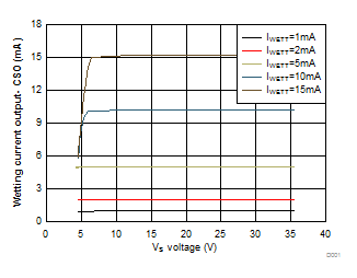
| TA = 25°C |
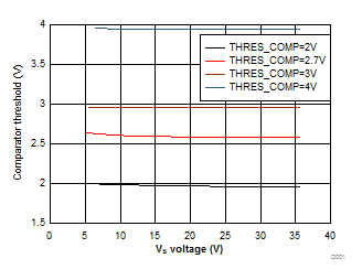
| TA = 25°C |
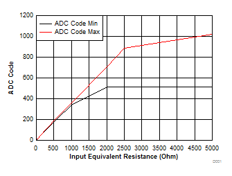
| I(WETT) = 2 mA | 6.5 V ≤ VS ≤ 35 V |
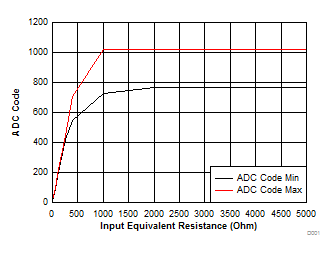
| I(WETT) = 10 mA | 6.5 V ≤ VS ≤ 35 V |
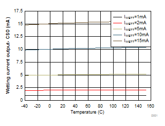
| VS = 12 V |
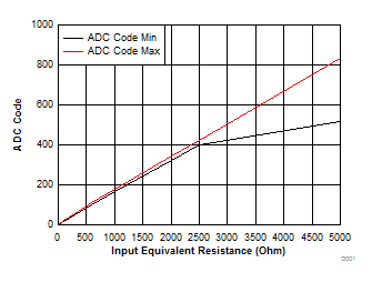
| I(WETT) = 1 mA | 6.5 V ≤ VS ≤ 35 V |
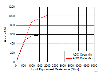
| I(WETT) = 5 mA | 6.5 V ≤ VS ≤ 35 V |
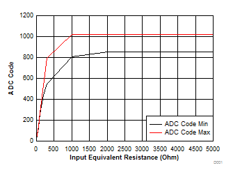
| I(WETT) = 15 mA | 6.5 V ≤ VS ≤ 35 V |