ZHCSK86 September 2019 THVD1505
PRODUCTION DATA.
8.3.1.1 Passive Polarity Definition Using Fail-Safe Biasing Network
Figure 18 shows a simple point-to-point data link between a master node and a slave node with mis-wire fault.
 Figure 18. Passive Polarity Definition
 During passive polarity definition, an external fail-safe resistor network (RFS) must be used to ensure fail-safe operation during an idle bus state. When the bus is not actively driven, the differential receiver inputs could float allowing the receiver output to assume a random output. A proper fail-safe network forces the receiver inputs to exceed the VIT threshold, thus forcing the THVD1505 receiver output into the high state.
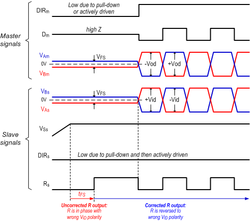
Figure 19 shows the timing diagram for passive polarity definition.
Prior to initiating data transmission the master transceiver must idle for a time span that exceeds the maximum fail-safe time, tFS, of a slave transceiver. This idle time is accomplished by driving the direction control line (the output of the MCU in Figure 19 that is driving DE and RE pins), DIR, low. After a time, t > tFS, the master begins transmitting data.
Because of the indicated mis-wire fault between master and slave, the slave node receives bus signals with reversed polarity. Assuming the slave node has just been connected to the bus, the direction-control pin is pulled-down during power-up and then is actively driven low by the slave MCU. The polarity correction begins as soon as the slave supply is established and ends after tFS.
 Figure 19. Polarity Correction Timing With Passive Polarity Definition
 Initially, the slave receiver assumes that the correct bus polarity is applied to the inputs and performs no polarity reversal. Because of the reversed polarity of the bus-failsafe voltage, the output of the slave receiver, RS, turns low. After tFS has passed and the receiver has detected the wrong bus polarity, the internal POLCOR logic reverses the input signal and RS turns high.
At this point, all incoming bus data with reversed polarity are polarity corrected within the transceiver. Because polarity correction is also applied to the transmit path, the data sent by the slave MCU are reversed by the POLCOR logic and then fed into the driver.
The reversed data from the slave MCU are reversed again by the mis-wire fault in the bus, and the correct bus polarity is reestablished at the master end.
THVD1505 retains the state of the polarity logic as long as VCC is present to the device. However, the device POLCOR logic powers up in the default no polarity reversal mode at each device power up. POLCOR logic remains active as long as VCC is applied to the device.
NOTE
Data string durations of consecutive 0s or 1s exceeding the minimum tFS can accidently trigger a wrong polarity correction and must be avoided.