SLOS776A September 2012 – December 2015 THS789
PRODUCTION DATA.
- 1 Features
- 2 Applications
- 3 Description
- 4 Revision History
- 5 Pin Configuration and Functions
- 6 Specifications
- 7 Detailed Description
- 8 Application and Implementation
- 9 Power Supply Recommendations
- 10Layout
- 11Device and Documentation Support
- 12Mechanical, Packaging, and Orderable Information
6 Specifications
6.1 Absolute Maximum Ratings
over operating junction temperature range (unless otherwise noted)| MIN | MAX | UNIT | |||
|---|---|---|---|---|---|
| VCC | 4 | V | |||
| Analog I/O to GND(2) | –0.3 | VCC + 0.3 | V | ||
| Digital I/O to GND | –0.3 | VCC + 0.3 | V | ||
| TJ | Maximum junction temperature(1) | 150 | °C | ||
| Tstg | Storage temperature | 150 | °C | ||
(1) The THS789 device has an automatic power shutdown at 140°C, typical.
(2) LVDS outputs are not short-circuit-proof to GND.
6.2 ESD Ratings
| VALUE | UNIT | ||||
|---|---|---|---|---|---|
| V(ESD) | Electrostatic discharge | Human body model (HBM), per ANSI/ESDA/JEDEC JS-001, all pins(1) | ±2000 | V | |
| Charged device model (CDM), per JEDEC specification JESD22-C101, all pins(2) | ±250 | ||||
(1) JEDEC document JEP155 states that 500-V HBM allows safe manufacturing with a standard ESD control process.
(2) JEDEC document JEP157 states that 250-V CDM allows safe manufacturing with a standard ESD control process.
6.3 Recommended Operating Conditions
over operating junction temperature range (unless otherwise noted)| MIN | NOM | MAX | UNIT | ||
|---|---|---|---|---|---|
| VCC | Supply voltage | 3.135 | 3.465 | V | |
| TJ | Junction temperature | 0 | 105 | °C | |
| MCLOCK frequency | 200 | MHz | |||
6.4 Thermal Information
| THERMAL METRIC(1) | THS789 | UNIT | |
|---|---|---|---|
| PFD (HTQFP) | |||
| 100 PINS | |||
| RθJA | Junction-to-ambient thermal resistance | 24.2 | °C/W |
| RθJC(top) | Junction-to-case (top) thermal resistance | 10.4 | °C/W |
| RθJB | Junction-to-board thermal resistance | 9.8 | °C/W |
| ψJT | Junction-to-top characterization parameter | 0.3 | °C/W |
| ψJB | Junction-to-board characterization parameter | 9.7 | °C/W |
| RθJC(bot) | Junction-to-case (bottom) thermal resistance | 0.5 | °C/W |
(1) For more information about traditional and new thermal metrics, see the Semiconductor and IC Package Thermal Metrics application report, SPRA953.
6.5 Electrical Characteristics
Typical conditions are at TJ = 55°C and VCC = 3.3 V.6.6 Host Serial Interface DC Characteristics
over operating junction temperature range (unless otherwise noted)| PARAMETER | TEST CONDITIONS | MIN | TYP | MAX | UNIT | |
|---|---|---|---|---|---|---|
| VIH | High-level input voltage | 0.7 × VCC | VCC + 0.5 | V | ||
| VIL | Low-level input voltage | GND – 0.3 | 0.3 × VCC | V | ||
| VOH | High-level output voltage | VCC – 0.5 | VCC + 0.3 | V | ||
| VOL | Low-level output voltage | 0 | 0.4 | V | ||
| Ilkg | Leakage current | 1 | µA | |||
6.7 Host Serial Interface AC Characteristics
over operating junction temperature range (unless otherwise noted)| PARAMETER | TEST CONDITIONS | MIN | TYP | MAX | UNIT |
|---|---|---|---|---|---|
| HCLK frequency | 50 | MHz | |||
| Rise and fall times | 3.5 | ns | |||
| HCLK duty cycle | 40% | 50% | 60% | ||
| Hstrobe high period between two consecutive transactions | 40 | ns | |||
| Hstrobe low to HCLK high setup | 5 | ns | |||
| HCLK high to Hstrobe high hold time | 5 | ns | |||
| Hdata in to HCLK high setup | 5 | ns | |||
| Hdata in to HCLK high hold time | 5 | ns | |||
| HCLK falling edge to Hdata out (L or H) | CL = 20 pF | 3.25 | ns | ||
| HCLK falling edge to Hdata out (H or L) | CL = 20 pF | 3.25 | ns |
6.8 Power Consumption
Typical conditions are at 55°C junction temperature, VCC = 3.3 V.| CONDITION | TYP | MAX | UNIT | |||
|---|---|---|---|---|---|---|
| Four channel current | 925 | 1236 | mA | |||
6.9 Typical Characteristics
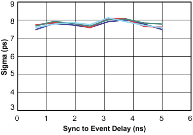
 Figure 1. Typical Per Channel Sigmas vs 5-ns (200-MHz) Window