SLOS776A September 2012 – December 2015 THS789
PRODUCTION DATA.
- 1 Features
- 2 Applications
- 3 Description
- 4 Revision History
- 5 Pin Configuration and Functions
- 6 Specifications
- 7 Detailed Description
- 8 Application and Implementation
- 9 Power Supply Recommendations
- 10Layout
- 11Device and Documentation Support
- 12Mechanical, Packaging, and Orderable Information
8 Application and Implementation
NOTE
Information in the following applications sections is not part of the TI component specification, and TI does not warrant its accuracy or completeness. TI’s customers are responsible for determining suitability of components for their purposes. Customers should validate and test their design implementation to confirm system functionality.
8.1 Application Information
The THS789 device is a high-speed, high-resolution time-measurement unit that measures the difference in time between a signal applied to an event channel and the signal applied to the sync channel. This difference is then transmitted to a result interface in the form of a digital word. Figure 6 shows an example of three time measurements (T1, T2, and T3).
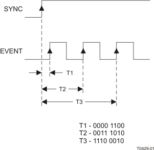 Figure 6. Time-Measurement Example With 8-Bit Words Triggered by Rising Edges
The previous time difference is calculated by an internal ALU that subtracts the timestamps created by the Event signal and the SYNC signal stored in a FIFO. These timestamps are performed by the TDC that is composed by the following: an interpolator, a synchronizer, a 34-bit counter, and a 1.2-GHz clock. It is important to note that the event and sync channels share the same TDC. When a valid edge is applied to the event channel, the TDC uses the value in the counter and stores it in the FIFO. Then the ALU uses the value of the event and the value of the sync, stored in the FIFO already, and subtracts them. After the operation is done, the final value is shifted out to the result interface for retrieval.
All the programming to the THS789 device is achieved through an LVCMOS host-serial interface. With this interface, the user has the ability to set up the THS789 device for time measurements. It also provides the user with different modes to retrieve the results.
Results are available through an LVDS-compatible high-speed serial interface. Data-word length and speed are programmable to cover a wide range of data rates. Each channel has it own output to maximize data throughput. All of the data ports (RdataA, -B, -C, and -D) are synchronized to a global clock.
8.2 Typical Application
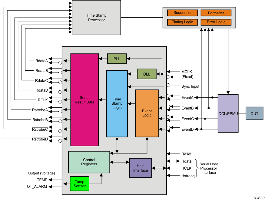 Figure 7. Example of Application Diagram in ATE Environment
8.2.1 Design Requirements
For this design example, use the parameters listed in Table 15 as the input parameters.
Table 15. Design Parameters
| DESIGN PARAMETER | EXAMPLE VALUE |
|---|---|
| Results interface size | 40 bit |
| Results time range | –7.158 to 7.158 s |
| Rclock | 300 MHz |
| DDR mode | Off |
| Temperature monitor | On |
| Connect CD/Connect AB | Off |
| Counter size | 34 bit |
| REGISTER WRITE (80h) | 0xA680 |
| REGISTER WRITE (81h) | 0x0003 |
8.2.2 Detailed Design Procedures
8.2.2.1 Time Measurement
Time measurements in the THS789 device follow the timing of Figure 8. This diagram illustrates that time measurements are valid as long as events do not happen at speeds higher than 200 MHz. If an event happens at less than 5 ns from the previous one, then this event is ignored. The same applies to the SYNC signal. Even though the minimum period is 5 ns, the pulse duration of both Event and SYNC signals can be as low as 200 ps.
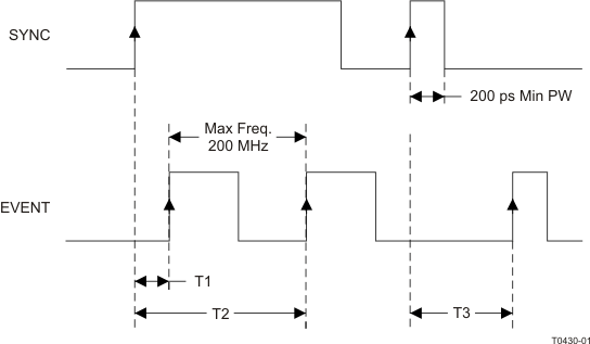 Figure 8. Time-Measurement Example at Maximum Retrigger Rate and Minimum Pulse Duration
The TH788 is capable of making time measurements using any combination of rising-falling edge between Event and SYNC. The example in Figure 8 uses rising edges only to trigger the time measurement. Table 16 describes what registers bits must be programmed to achieve the desired combination. Registers to be programmed are 00h, 20h, 40h, and 60h for event channels and 80h for the sync channel. The examples in Figure 9 illustrate the other three combinations. All of the channels can be programmed individually with respect to the sync channel.
Table 16. Trigger Polarity Programmability
| REGISTER BITS | TRIGGER POLARITY FROM SYNC TO EVENT |
|
|---|---|---|
| SYNC_TS_Pol | Pol_X | |
| 0 | 0 | Pos to Pos |
| 0 | 1 | Pos to Neg |
| 1 | 0 | Neg to Pos |
| 1 | 1 | Neg to Neg |
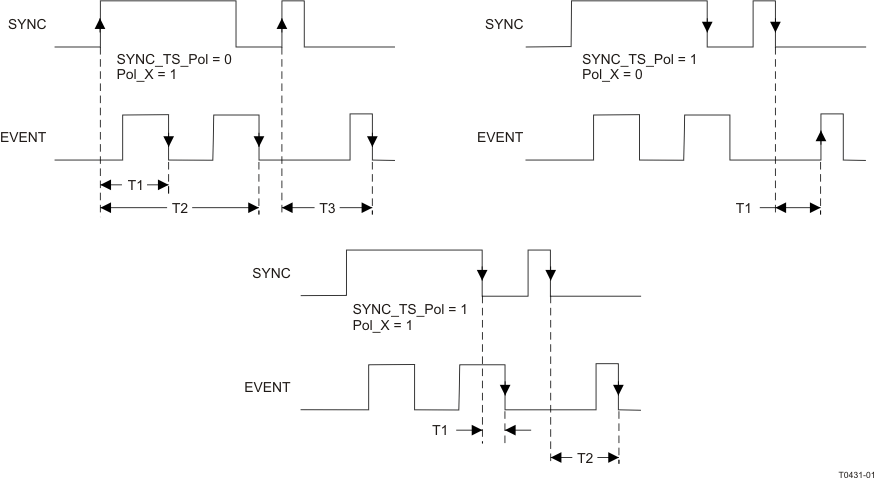 Figure 9. Time-Measurement Examples With Different Edge Polarities
8.2.2.2 Output Clock to Data/Strobe Phasing
The output of each channel is an Rdata and Rstrobe signal. The RCLK for all the channels is a common output. Operating at 300 MHz, these signals must be handled carefully. Particularly important are the termination and phase alignment of the signals at the receiving circuitry. Termination has been discussed previously. Phase alignment is now discussed: The two outputs from each channel are clocked out through identical flip-flops with the same internal clock. Data and strobe output edges from a particular channel match well (< 50 ps). The match channel-to-channel is not as good due to the greater wiring distances internal to the TMU. However, the total time difference is below 125 ps. Because the RClock is a common output, the wiring lengths from the four channels must be matched and controlled to achieve good setup and hold times at the input to the receiving circuit. The RClock rising edge is adjusted internal to the TMU to be close to the center of the eye diagram of the data/strobe signals. (The internal clock has a good 50/50 duty cycle. The rising edge clocks out the data/strobe. The falling edge is inverted and used as the RClock after appropriate adjustments for the internal propagation delay times.) The receiving circuitry requirements for setup and hold timing must be carefully examined for the proper timing. Delays may be added to the PCB microstrips to adjust timing. A good rule is 125 ps of delay per inch of microstrip length.
8.2.2.3 Master Clock Input and Clock Multiplier
All of the internal timing of the TMU is derived from the 200-MHz master clock. Therefore, its quality is critical to the accurate operation of the TMU. Absolute accuracy of the master clock linearly affects the accuracy of the measurements. This imposes little burden upon the master clock, as accurate oscillators are easy to procure or distribute. However, the jitter of the master clock is also highly critical to the single-event precision of the TMU and should be absolutely minimized (< 3-ps RMS). A carefully selected crystal oscillator can meet this requirement. However, jitter can build up quite quickly in a clock distribution scheme and must be carefully controlled. Be careful that the LVDS input to the master clock is not badly distorted or that the rise and fall times are slow (> 0.6 ns).
Discussion of the clock multiplier follows: The TMU operates from a master-clock frequency of 1200 MHz, which implies a measurement period of 0.833 ns. The master counter runs from this frequency, and all the other clocks are divided down from this main clock. An interpolator allows finer precision in time measurement, as discussed elsewhere. The clock multiplier is the circuit that takes the 200-MHz master-clock reference and generates from that the high quality 1200-MHz clock. The clock multiplier consists of five major sections: First is the delay-lock loop (DLL), which is a series connection of 12 identical and closely matched variable time-delay circuits. A single control voltage connects to each of the delay elements. The master 200-MHz clock connects to the input of the DLL. Because the period of 200 MHz is 5 ns, if the control voltage is adjusted to make the time delay of the DLL equal to 5 ns, the input and the output of the delay line is exactly phase matched. A phase detector connected to the input and the output of the delay line can sense this condition accurately, and a feedback loop with a low-offset-error amplifier is included in the clock multiplier to achieve this result. These are the second and third circuit blocks. With 12 equally spaced 200-MHz clock phases, select out six equally spaced 833-ps-wide pulses with AND gates and combine these pulses into a single 1200-MHz clock waveform with a six-input OR gate. The last circuit element is a powerful differential signal buffer to distribute the 1200-MHz clock to the various circuit elements in the TMU. The DLL feedback loop is fairly narrowband, so some time is required to allow the DLL to initialize at start-up (about 100 μs, typical). The DLL is insensitive to the duty cycle of the input 200-MHz clock. Duty cycles of 40/60 to 60/40 are acceptable. What matters most is as little jitter as possible.
8.2.2.4 Temperature Measurement and Alarm Circuit
Chip temperature of the TMU is monitored by a temperature sensor located near the center of the chip. A small buffer outputs a voltage proportional to the absolute temperature of the TMU. The buffer drives a load of up to 100 pF typical (50 pF minimum) and open circuit to 10 kΩ to ground resistive. The output voltage slope is 5 mV, typical. Therefore, the output voltage equation is as follows:
Also included in the TMU is an overtemperature comparator. At approximately 140°C, the alarm goes active, and at approximately 7°C below this temperature, the alarm becomes inactive (hysteresis of 7°C prevents tripping on noise and comparator oscillations). If the alarm goes active, the chip powers down and sets a bit in the serial register.
An alarm output pin is provided that is an open-drain output. Connect this output through a pullup resistor to the 3.3-V power supply. The resistor must be at least 3.3 kΩ. This creates a slow-speed, low-voltage CMOS digital output with a logical 1 being the normal operating state and a logical 0 being the overtemperature state.
8.2.2.5 LVDS-Compatible I/Os
The Event, SYNC, and master-clock inputs are LVDS-compatible input receivers optimized for high-speed and low-time-distortion operation. The Rdata, Rstrobe, and RCLK outputs are similarly LVDS-compatible output drivers optimized for high-speed/low-distortion operation, driving 50-Ω transmission lines. Typically, LVDS data transmission is thought of in terms of 100-Ω twisted-wire-pair (TWP) transmission lines. TWP is not applicable to printed wiring boards and high-speed operation. Therefore, the THS789 device interfaces were designed to operate most effectively with 50-Ω, single-ended transmission lines. Instead of a current-mode output with its correspondingly high output impedance, a more-nearly impedance-matched voltage-mode output driver is used. This minimizes reflections from mismatched transmission line terminations and the resulting waveform distortion. The input receivers do not include the 100-Ω terminating resistor, which must be connected externally to the THS789 device. This was done to accommodate daisy-chaining the THS789 inputs. Input offset voltage was minimized, and the fail-safe feature in the LVDS standard was eliminated in order to minimize distortion.
8.2.2.6 LVDS-Compatible Inputs
The four event inputs, the sync input and the master-clock input all use the same input interface circuitry. Figure 10 is a simplified schematic diagram of the LVDS-compatible receiver input stage. The input signal is impedance-transformed and level-shifted with a PNP emitter-follower and translated into ECL-like differential signals with a common-emitter amplifier. There is no internal termination resistor and no internal pullup or pulldown resistors. Unused inputs may be tied off by connecting both input terminals to ground. If the input terminals are left floating, they are protected by ESD clamps from damage; however, noise may be injected into the THS789 device and may degrade accuracy. The peak input voltage limits are 0.6 V to 1.7 V. Outside of these limiting voltages, parts of the input circuit may saturate and distort the timing.
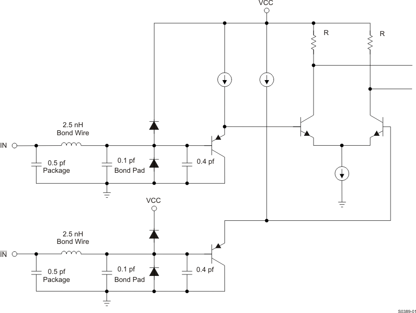 Figure 10. Simplified Schematic of the LVDS Input
Figure 11 shows the typical input connections. The transmission line lengths must be matched from the driver to the THS789 input [< 0.5 inch (1.27 cm) difference] and terminated in a 100-Ω resistor placed close [< 0.25 inch (0.635 cm)] to the TMU input pins. The resistor total tolerance should be below 5%. The power dissipation is below 5 mW, so small surface-mounted resistors are preferred.
 Figure 11. Typical Input Connection to the THS789
8.2.2.7 LVDS-Compatible Outputs
Figure 12 shows a typical wiring diagram of an LVDS output. The transmission line lengths must be matched. A termination resistor may be required if the chosen receiver does not have an internal resistor. Concerning termination resistors: LVDS was originally conceived with twisted-wire pairs of approximately 100-Ω line-to-line impedance. The 100-Ω resistor between lines is simple and effective to terminate such a line. For the higher-speed operation of the THS789 device, use a pair of 50-Ω transmission lines, such as microstrip on the PC board. The same 100-Ω resistor line-to-line termination works well, because the line signals are equal and opposite in phase. This results in the center of the 100-Ω resistor having a constant voltage equal to the common-mode voltage and each side having an apparent 50-Ω termination. An improvement in the termination can be achieved by splitting the 100 Ω into two 50-Ω resistors and ac-grounding (bypassing) the center to ground with a 1000-pF (not critical) capacitor. The termination improvement is usually small and increases the room and parts count. It is the best approach as long as the PCB layout high-frequency performance is not compromised by the higher parts count. As mentioned previously, the driver is optimized to drive 50-Ω transmission lines and provides a driving-point impedance approximating 50 Ω to suppress reflections. Figure 8 is a simplified schematic of the output driver. A standard ECL-like circuit drives the outputs through 25-Ω resistors. The combination of the resistors and the emitter-follower output impedance approximates 50 Ω. The output emitter-followers are biased by current sources that are switched to conserve power. A feedback loop varies the voltage on the two RLs to set and maintain the 1.28-V common-mode voltage of the LVDS-compatible outputs. Another feedback loop holds the emitters of the current switches to 0.4 V to keep the 4-mA current source from saturation.
The outputs are short-circuit-proof to a 3.3-V power supply. Shorts to ground should be avoided, as the power dissipation in certain components may exceed safe limits.
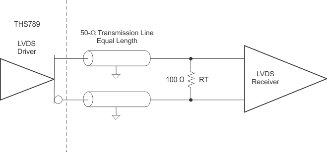 Figure 12. Typical Output Connection to the THS789
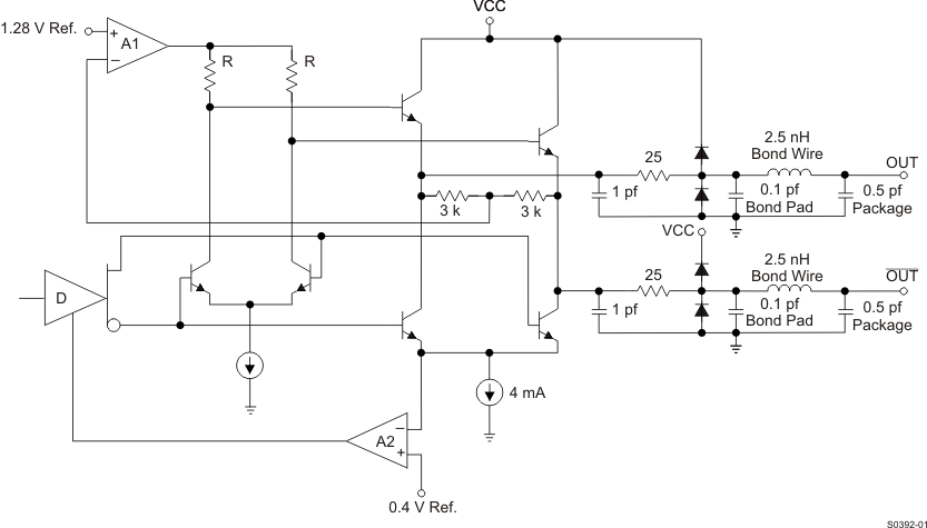 Figure 13. Simplified Schematic of the LVDS Output Driver
8.2.3 Application Curve
 Figure 14. 4-Channel Supply Current vs Rdata, Counter, and Rclock Functional Modes