ZHCSRC5K september 2003 – april 2023 THS3091 , THS3095
PRODUCTION DATA
- 1 特性
- 2 应用
- 3 描述
- 4 Revision History
- 5 Device Comparison Table
- 6 Pin Configuration and Functions
- 7 Specifications
- 8 Detailed Description
- 9 Application and Implementation
- 10Device and Documentation Support
- 11Mechanical, Packaging, and Orderable Information
封装选项
机械数据 (封装 | 引脚)
散热焊盘机械数据 (封装 | 引脚)
订购信息
8.4.1 Wideband, Noninverting Operation
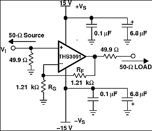
The THS309x are unity gain stable 715-MHz current-feedback operational amplifiers designed to operate from a ±5-V to ±15-V power supply. Figure 8-2 shows the THS3091 in a noninverting gain of 2-V/V configuration typically used to generate the performance curves. Most of the curves were characterized using signal sources with a 50-Ω source impedance, and with measurement equipment presenting a 50-Ω load impedance.
 Figure 8-2 Wideband, Noninverting Gain Configuration
Current-feedback amplifiers are highly dependent on feedback resistor RF for maximum performance and stability. Table 8-1 shows the optimal gain-setting resistors RF and RG at different gains to give maximum bandwidth with minimal peaking in the frequency response. Higher bandwidths can be achieved (at the expense of added peaking in the frequency response) by using even lower values for RF. Conversely, increasing RF decreases the bandwidth, but improves stability.
| THS3091 AND THS3095 RF AND RG VALUES FOR MINIMAL PEAKING WITH RL = 100 Ω | |||
|---|---|---|---|
| GAIN (V/V) | SUPPLY VOLTAGE (V) | RG (Ω) | RF (Ω) |
| 1 | ±5 and ±15 | — | 1.78 k |
| 2 | ±5 | 1.15 k | 1.15 k |
| ±15 | 1.21 k | 1.21 k | |
| 5 | ±5 and ±15 | 249 | 1 k |
| 10 | ±5 and ±15 | 95.3 | 866 |
| –1 | ±5 and ±15 | 1.05 k | 1.05 k |
| –2 | ±5 and ±15 | 499 | 1 k |
| –5 | ±5 and ±15 | 182 | 909 |
| –10 | ±5 and ±15 | 86.6 | 866 |