ZHCSP01 July   2022 TCAL9539

ADVANCE INFORMATION  

  1. 特性
  2. 应用
  3. 说明
  4. Revision History
  5. Pin Configuration and Functions
  6. Specifications
    1. 6.1 Absolute Maximum Ratings
    2. 6.2 ESD Ratings
    3. 6.3 Recommended Operating Conditions
    4. 6.4 Thermal Information
    5. 6.5 Electrical Characteristics
    6. 6.6 Timing Requirements
    7. 6.7 I2C Bus Timing Requirements
    8. 6.8 Switching Characteristics
  7. Parameter Measurement Information
  8. Detailed Description
    1. 8.1 Overview
    2. 8.2 Functional Block Diagrams
    3. 8.3 Feature Description
      1. 8.3.1 I/O Port
      2. 8.3.2 Adjustable Output Drive Strength
      3. 8.3.3 Interrupt Output (INT)
      4. 8.3.4 Reset Input (RESET)
      5. 8.3.5 Software Reset Call
    4. 8.4 Device Functional Modes
      1. 8.4.1 Power-On Reset
    5. 8.5 Programming
      1. 8.5.1 I2C Interface
    6. 8.6 Register Maps
      1. 8.6.1 Device Address
      2. 8.6.2 Control Register and Command Byte
      3. 8.6.3 Register Descriptions
      4. 8.6.4 Bus Transactions
        1. 8.6.4.1 Writes
        2. 8.6.4.2 Reads
  9. Application and Implementation
    1. 9.1 Application Information
    2. 9.2 Typical Application
      1. 9.2.1 Design Requirements
      2. 9.2.2 Detailed Design Procedure
        1. 9.2.2.1 Minimizing ICC When I/Os Control LEDs
      3. 9.2.3 Application Curves
    3. 9.3 Power Supply Recommendations
      1. 9.3.1 Power-On Reset Requirements
    4. 9.4 Layout
      1. 9.4.1 Layout Guidelines
      2. 9.4.2 Layout Example
  10. 10Device and Documentation Support
    1. 10.1 接收文档更新通知
    2. 10.2 支持资源
    3. 10.3 Trademarks
    4. 10.4 Electrostatic Discharge Caution
    5. 10.5 术语表
  11. 11Mechanical, Packaging, and Orderable Information
    1. 11.1 Tape and Reel Information
    2. 11.2 Mechanical Data

封装选项

机械数据 (封装 | 引脚)
散热焊盘机械数据 (封装 | 引脚)
订购信息

Detailed Design Procedure

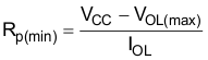
The pull-up resistors, RP, for the SCL and SDA lines need to be selected appropriately and take into consideration the total capacitance of all responders on the I2C bus. The minimum pull-up resistance is a function of VCC, VOL,(max), and IOL:

Equation 1. GUID-DD6FD861-B884-4ED8-BFC3-8865FCBAEA66-low.gif

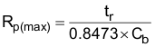
The maximum pull-up resistance is a function of the maximum rise time, tr (120 ns for fast-mode-plus operation, fSCL = 1 MHz) and bus capacitance, Cb:

Equation 2. GUID-D69A514A-196C-4378-BA0C-161D7A3FE943-low.gif

The maximum bus capacitance for an I2C bus must not exceed 400 pF for standard-mode or fast-mode operation, or 550pF for fast-mode-plus. The bus capacitance can be approximated by adding the capacitance of the TCAL9539, Ci for SCL or Cio for SDA, the capacitance of wires/connections/traces, and the capacitance of additional responders on the bus.