ZHCS290G September 2009 – June 2018 TCA8418
PRODUCTION DATA.
- 1 特性
- 2 应用范围
- 3 说明
- 4 修订历史记录
- 5 Pin Configuration and Functions
-
6 Specifications
- 6.1 Absolute Maximum Ratings
- 6.2 ESD Ratings
- 6.3 Recommended Operating Conditions
- 6.4 Thermal Information
- 6.5 Electrical Characteristics
- 6.6 I2C Interface Timing Requirements
- 6.7 Reset Timing Requirements
- 6.8 Switching Characteristics
- 6.9 Keypad Switching Characteristics
- 6.10 Typical Characteristics
- 7 Parameter Measurement Information
-
8 Detailed Description
- 8.1 Overview
- 8.2 Functional Block Diagram
- 8.3 Feature Description
- 8.4 Device Functional Modes
- 8.5 Programming
- 8.6
Register Maps
- 8.6.1 Device Address
- 8.6.2
Control Register and Command Byte
- 8.6.2.1 Configuration Register (Address 0x01)
- 8.6.2.2 Interrupt Status Register, INT_STAT (Address 0x02)
- 8.6.2.3 Key Lock and Event Counter Register, KEY_LCK_EC (Address 0x03)
- 8.6.2.4 Key Event Registers (FIFO), KEY_EVENT_A–J (Address 0x04–0x0D)
- 8.6.2.5 Keypad Lock1 to Lock2 Timer Register, KP_LCK_TIMER (Address 0x0E)
- 8.6.2.6 Unlock1 and Unlock2 Registers, UNLOCK1/2 (Address 0x0F-0x10)
- 8.6.2.7 GPIO Interrupt Status Registers, GPIO_INT_STAT1–3 (Address 0x11–0x13)
- 8.6.2.8 GPIO Data Status Registers, GPIO_DAT_STAT1–3 (Address 0x14–0x16)
- 8.6.2.9 GPIO Data Out Registers, GPIO_DAT_OUT1–3 (Address 0x17–0x19)
- 8.6.2.10 GPIO Interrupt Enable Registers, GPIO_INT_EN1–3 (Address 0x1A–0x1C)
- 8.6.2.11 Keypad or GPIO Selection Registers, KP_GPIO1–3 (Address 0x1D–0x1F)
- 8.6.2.12 GPI Event Mode Registers, GPI_EM1–3 (Address 0x20–0x22)
- 8.6.2.13 GPIO Data Direction Registers, GPIO_DIR1–3 (Address 0x23–0x25)
- 8.6.2.14 GPIO Edge/Level Detect Registers, GPIO_INT_LVL1–3 (Address 0x26–0x28)
- 8.6.2.15 Debounce Disable Registers, DEBOUNCE_DIS1–3 (Address 0x29–0x2B)
- 8.6.2.16 GPIO pull-up Disable Register, GPIO_PULL1–3 (Address 0x2C–0x2E)
- 8.6.3 CAD Interrupt Errata
- 8.6.4 Overflow Errata
- 9 Application and Implementation
- 10Power Supply Recommendations
- 11Layout
- 12器件和文档支持
- 13机械、封装和可订购信息
9.2.2.1 Designing the Hardware Layout
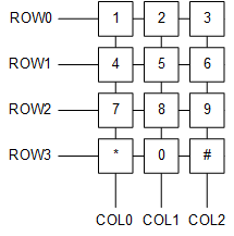
The first steps towards designing a keypad array is to determine the desired layout, and to map each key to the appropriate value which will show up in the FIFO. For this example, the number pad below is the physical location of the keys that are desired. The layout is a 4 x 3 array, using rows 0-3 and columns 0-2. For this example, we will not assume any of the other pins will be used.
The following behavior is desired for this example design
- All keys in the keypad array to be added to the FIFO upon a key press
- Attempting to clear the interrupt before the proper registers have been cleared to de-assert the INT pin for 50 μs, then assert the INT pin.
- No additional pins are being used, other than the keypad array
- Keypad lock support, requiring that the unlock combination be ‘#, 1’ which must be pressed within 2 seconds of each other
- Keypad lock interrupt mask timer of 10 seconds to match the back light auto-turn off with 10 seconds of no interrupt
- Hardware debouncing to be enabled
 Figure 30. Example Keypad
 Since the TCA8418 reports keys pressed according to the values in the key value table, it is important to know the TCA8418 values for the key locations.
According to the key event table, the key presses are assigned in Table 12.
Table 12. Key Press Assignment
| Keypad Button | 1 | 2 | 3 | 4 | 5 | 6 | 7 | 8 | 9 | * | 0 | # |
| Key Event Table Value (Decimal) | 1 | 2 | 3 | 11 | 12 | 13 | 21 | 22 | 23 | 31 | 32 | 33 |
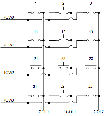
The schematic for this keypad layout is shown in figure (schematic below) with the key event table values. Note that no external pullup resistors are needed, because the TCA8418 has integrated pullup resistors.
 Figure 31. Keypad Schematic