SLOS838C July 2013 – August 2015 TAS5731M
PRODUCTION DATA.
- 1 Features
- 2 Applications
- 3 Description
- 4 Revision History
- 5 Device Comparison Table
- 6 Pin Configuration and Functions
-
7 Specifications
- 7.1 Absolute Maximum Ratings
- 7.2 ESD Ratings
- 7.3 Recommended Operating Conditions
- 7.4 Thermal Information
- 7.5 PWM Operation at Recommended Operating Conditions
- 7.6 DC Electrical Characteristics
- 7.7 AC Electrical Characteristics (BTL, PBTL)
- 7.8 Electrical Characteristics - PLL External Filter Components
- 7.9 Electrical Characteristic - I2C Serial Control Port Operation
- 7.10 Timing Requirements - PLL Input Parameters
- 7.11 Timing Requirements - Serial Audio Ports Slave Mode
- 7.12 Timing Requirements - I2C Serial Control Port Operation
- 7.13 Timing Requirements - Reset (RESET)
- 7.14 Typical Characteristics
- 8 Parameter Measurement Information
-
9 Detailed Description
- 9.1 Overview
- 9.2 Functional Block Diagrams
- 9.3
Feature Description
- 9.3.1 Power Supply
- 9.3.2 I2C Address Selection and Fault Output
- 9.3.3 Single-Filter PBTL Mode
- 9.3.4 Device Protection System
- 9.3.5 SSTIMER Functionality
- 9.3.6 Clock, Autodetection, and PLL
- 9.3.7 PWM Section
- 9.3.8 2.1-Mode Support
- 9.3.9 I2C Compatible Serial Control Interface
- 9.3.10 Audio Serial Interface
- 9.3.11 Dynamic Range Control (DRC)
- 9.4 Device Functional Modes
- 9.5 Programming
- 9.6
Register Maps
- 9.6.1 Clock Control Register (0x00)
- 9.6.2 Device ID Register (0x01)
- 9.6.3 Error Status Register (0x02)
- 9.6.4 System Control Register 1 (0x03)
- 9.6.5 Serial Data Interface Register (0x04)
- 9.6.6 System Control Register 2 (0x05)
- 9.6.7 Soft Mute Register (0x06)
- 9.6.8 Volume Registers (0x07, 0x08, 0x09, 0x0A)
- 9.6.9 Volume Configuration Register (0x0E)
- 9.6.10 Modulation Limit Register (0x10)
- 9.6.11 Interchannel Delay Registers (0x11, 0x12, 0x13, and 0x14)
- 9.6.12 PWM Shutdown Group Register (0x19)
- 9.6.13 Start/Stop Period Register (0x1A)
- 9.6.14 Oscillator Trim Register (0x1B)
- 9.6.15 BKND_ERR Register (0x1C)
- 9.6.16 Input Multiplexer Register (0x20)
- 9.6.17 Channel 4 Source Select Register (0x21)
- 9.6.18 PWM Output Mux Register (0x25)
- 9.6.19 DRC Control Register (0x46)
- 9.6.20 Bank Switch and EQ Control Register (0x50)
-
10Application and Implementation
- 10.1 Application Information
- 10.2
Typical Applications
- 10.2.1 Stereo Bridge Tied Load Application
- 10.2.2 Mono Parallel Bridge Tied Load Application
- 10.2.3 2.1 Application
- 11Power Supply Recommendations
- 12Layout
- 13Device and Documentation Support
- 14Mechanical, Packaging, and Orderable Information
7 Specifications
7.1 Absolute Maximum Ratings
over operating free-air temperature range (unless otherwise noted) (1)| MIN | MAX | UNIT | ||
|---|---|---|---|---|
| Supply voltage | DVDD, AVDD | –0.3 | 4.2 | V |
| PVDD_x | –0.3 | 30 | V | |
| Input voltage | 3.3-V digital input | –0.5 | DVDD + 0.5 | V |
| 5-V tolerant(2) digital input (except MCLK) | –0.5 | DVDD + 2.5(4) | ||
| 5-V tolerant MCLK input | –0.5 | AVDD + 2.5(4) | ||
| OUT_x to PGND_x | 32(3) | V | ||
| BST_x to PGND_x | 39(3) | V | ||
| Input clamp current, IIK | –20 | 20 | mA | |
| Output clamp current, IOK | –20 | 20 | mA | |
| Operating free-air temperature | 0 | 85 | °C | |
| Operating junction temperature | 0 | 150 | °C | |
| Storage temperature, Tstg | –40 | 125 | °C | |
(1) Stresses beyond those listed under Absolute Maximum Ratings may cause permanent damage to the device. These are stress ratings only and functional operation of the device at these or any other conditions beyond those indicated under Recommended Operating Conditions is not implied. Exposure to absolute-maximum conditions for extended periods may affect device reliability.
(2) 5-V tolerant inputs are PDN, RESET, SCLK, LRCLK, MCLK, SDIN, SDA, and SCL.
(3) DC voltage + peak ac waveform measured at the pin must be below the allowed limit for all conditions.
(4) Maximum pin voltage must not exceed 6 V.
7.2 ESD Ratings
| VALUE | UNIT | |||
|---|---|---|---|---|
| V(ESD) | Electrostatic discharge | Human body model (HBM), per ANSI/ESDA/JEDEC JS-001(1) | ±1000 | V |
| Charged-device model (CDM), per JEDEC specification JESD22-C101(2) | ±250 | |||
(1) JEDEC document JEP155 states that 500-V HBM allows safe manufacturing with a standard ESD control process.
(2) JEDEC document JEP157 states that 250-V CDM allows safe manufacturing with a standard ESD control process.
7.3 Recommended Operating Conditions
| MIN | NOM | MAX | UNIT | |||
|---|---|---|---|---|---|---|
| Digital/analog supply voltage | DVDD, AVDD | 3 | 3.3 | 3.6 | V | |
| Half-bridge supply voltage | PVDD_x | 8 | 26.4(2) | V | ||
| VIH | High-level input voltage | 5-V tolerant | 2 | V | ||
| VIL | Low-level input voltage | 5-V tolerant | 0.8 | V | ||
| TA | Operating ambient temperature range | 0 | 85 | °C | ||
| TJ(1) | Operating junction temperature range | 0 | 125 | °C | ||
| RL (PBTL) | Load impedance | Output filter: L = 15 μH, C = 680 nF | 2 | Ω | ||
| RL (BTL) | Load impedance | Output filter: L = 15 μH, C = 680 nF | 4 | Ω | ||
| RL (SE) | Load impedance | Output filter: L = 15 μH, C = 680 nF | 2 | Ω | ||
| LO | Output-filter inductance | Minimum output inductance under short-circuit condition | 10 | μH | ||
(1) Continuous operation above the recommended junction temperature may result in reduced reliability and/or lifetime of the device.
(2) For operation at PVDD_x levels greater than 18 V, the modulation limit must be set to 93.8% through the control port register 0x10.
7.4 Thermal Information
| THERMAL METRIC(1) | TAS5731M | UNIT | |
|---|---|---|---|
| PHP (HTQFP) | |||
| 48 PINS | |||
| RθJA | Junction-to-ambient thermal resistance | 27.9 | °C/W |
| RθJC(top) | Junction-to-case (top) thermal resistance | 1.1 | °C/W |
| RθJB | Junction-to-board thermal resistance | 13 | °C/W |
| ψJT | Junction-to-top characterization parameter | 20.7 | °C/W |
| ψJB | Junction-to-board characterization parameter | 0.3 | °C/W |
| RθJC(bot) | Junction-to-case (bottom) thermal resistance | 6.7 | °C/W |
(1) For more information about traditional and new thermal metrics, see the Semiconductor and IC Package Thermal Metrics application report, SPRA953.
7.5 PWM Operation at Recommended Operating Conditions
| PARAMETER | TEST CONDITIONS | VALUE | UNIT |
|---|---|---|---|
| Output PWM switch frequency | 11.025/22.05/44.1-kHz data rate ±2% | 352.8 | kHz |
| 48/24/12/8/16/32-kHz data rate ±2% | 384 |
7.6 DC Electrical Characteristics
TA = 25°, PVDD_x = 18 V, DVDD = AVDD = 3.3 V, RL= 8 Ω, BTL AD mode, fS = 48 kHz (unless otherwise noted)| PARAMETER | TEST CONDITIONS | MIN | TYP | MAX | UNIT | ||
|---|---|---|---|---|---|---|---|
| VOH | High-level output voltage | ADR/FAULT and SDA | IOH = –4 mA DVDD = 3 V |
2.4 | V | ||
| VOL | Low-level output voltage | ADR/FAULT and SDA | IOL = 4 mA DVDD = 3 V |
0.5 | V | ||
| IIL | Low-level input current | VI < VIL; DVDD = AVDD = 3.6 V |
75 | μA | |||
| IIH | High-level input current | VI > VIH; DVDD = AVDD = 3.6 V |
75(3) | μA | |||
| IDD | 3.3-V supply current | 3.3-V supply voltage (DVDD, AVDD) | Normal mode | 49 | 68 | mA | |
| Reset (RESET = low, PDN = high) | 23 | 38 | |||||
| IPVDD | Supply current | No load (PVDD_x) | Normal mode | 32 | 50 | mA | |
| Reset (RESET = low, PDN = high) | 4 | 8 | |||||
| rDS(on)(2) | Drain-to-source resistance, LS | TJ = 25°C, includes metallization resistance | 80 | mΩ | |||
| Drain-to-source resistance, HS | TJ = 25°C, includes metallization resistance | 80 | |||||
| I/O PROTECTION | |||||||
| Vuvp | Undervoltage protection limit | PVDD falling | 6.4 | V | |||
| Vuvp,hyst | Undervoltage protection limit | PVDD rising | 7.1 | V | |||
| OTE(1) | Overtemperature error | 150 | °C | ||||
| OTEHYST(1) | Extra temperature drop required to recover from error | 30 | °C | ||||
| IOC | Overcurrent limit protection | Output to output short in BTL mode | 4.5 | A | |||
| IOCT | Overcurrent response time | 150 | ns | ||||
(1) Specified by design.
(2) This does not include bond-wire or pin resistance.
(3) IIH for the PBTL pin has a maximum limit of 200 µA due to an internal pulldown on the pin.
7.7 AC Electrical Characteristics (BTL, PBTL)
PVDD_x = 18 V, BTL AD mode, fS = 48 kHz, RL = 8 Ω, CBST = 10 nF, audio frequency = 1 kHz, AES17 filter,fPWM = 384 kHz, TA = 25°C (unless otherwise noted). All performance is in accordance with recommended operating conditions (unless otherwise noted).
| PARAMETER | TEST CONDITIONS | MIN | TYP | MAX | UNIT | |
|---|---|---|---|---|---|---|
| PO | Power output per channel | BTL mode, PVDD = 8 V, RL = 8 Ω, 7% THD | 3.9 | W | ||
| BTL mode, PVDD = 8 V, RL = 8 Ω,10% THD | 4.2 | |||||
| BTL mode, PVDD = 12 V, RL = 8 Ω, 7% THD | 8 | |||||
| BTL mode, PVDD = 12 V, RL = 8 Ω,10% THD | 9.6 | |||||
| BTL mode, PVDD = 18 V, RL = 8 Ω, 7% THD | 18.7 | |||||
| BTL mode, PVDD = 18 V, RL = 8 Ω, 10% THD | 21.2 | |||||
| BTL mode, PVDD = 24 V, RL = 8 Ω, 7% THD | 32.6 | |||||
| BTL mode, PVDD = 24 V, RL = 8 Ω, 10% THD | 37.2 | |||||
| PBTL mode, PVDD = 12 V, RL = 4 Ω, 7% THD | 16.5 | |||||
| PBTL mode, PVDD = 12 V, RL = 4 Ω, 10% THD | 17.9 | |||||
| PBTL mode, PVDD = 18 V, RL = 4 Ω, 7% THD | 37 | |||||
| PBTL mode, PVDD = 18 V, RL = 4 Ω, 10% THD | 39.6 | |||||
| PBTL mode, PVDD = 24 V, RL = 4 Ω, 10% THD | 66 | |||||
| PBTL mode, PVDD = 24 V, RL = 4 Ω, 10% THD | 69.6 | |||||
| SE Mode, PVDD = 12 V, RL = 4 Ω, 7% THD | 4.2 | |||||
| SE Mode, PVDD = 12 V, RL = 4 Ω, 10% THD | 4.6 | |||||
| SE Mode, PVDD = 18 V, RL = 4 Ω, 7% THD | 9.6 | |||||
| SE Mode, PVDD = 18 V, RL = 4 Ω, 10% THD | 10.2 | |||||
| SE Mode, PVDD = 24 V, RL = 4 Ω, 7% THD | 17.1 | |||||
| SE Mode, PVDD = 24 V, RL = 4 Ω, 10% THD | 18.1 | |||||
| THD+N | Total harmonic distortion + noise | PVDD = 8 V, PO = 1 W | 0.15% | |||
| PVDD = 12 V, PO = 1 W | 0.03% | |||||
| PVDD = 18 V, PO = 1 W | 0.04% | |||||
| PVDD = 24 V, PO = 1 W | 0.1% | |||||
| Vn | Output integrated noise (rms) | A-weighted | 46 | μV | ||
| Cross-talk | PO = 0.25 W, f = 1 kHz (AD Mode) | –67 | dB | |||
| SNR | Signal-to-noise ratio(1) | A-weighted, f = 1 kHz, maximum power at THD < 1% |
104 | dB | ||
(1) SNR is calculated relative to 0-dBFS input level.
7.8 Electrical Characteristics - PLL External Filter Components
| PARAMETER | TEST CONDITIONS | MIN | TYP | MAX | UNIT | |
|---|---|---|---|---|---|---|
| External PLL filter capacitor C1 | SMD 0603 X7R | 47 | nF | |||
| External PLL filter capacitor C2 | SMD 0603 X7R | 4.7 | nF | |||
| External PLL filter resistor R | SMD 0603, metal film | 470 | Ω | |||
7.9 Electrical Characteristic - I2C Serial Control Port Operation
for I2C Interface signals over recommended operating conditions (unless otherwise noted)| PARAMETER | TEST CONDITIONS | MIN | TYP | MAX | UNIT | |
|---|---|---|---|---|---|---|
| CL | Load capacitance for each bus line | 400 | pF | |||
7.10 Timing Requirements - PLL Input Parameters
| PARAMETER | TEST CONDITIONS | MIN | TYP | MAX | UNIT | |
|---|---|---|---|---|---|---|
| fMCLKI | MCLK frequency | 2.8224 | 24.576 | MHz | ||
| MCLK duty cycle | 40% | 50% | 60% | |||
| tr/tf(MCLK) | Rise/fall time for MCLK | 5 | ns | |||
| LRCLK allowable drift before LRCLK reset | 4 | MCLKs | ||||
7.11 Timing Requirements - Serial Audio Ports Slave Mode
over recommended operating conditions (unless otherwise noted)| PARAMETER | TEST CONDITIONS | MIN | TYP | MAX | UNIT | |
|---|---|---|---|---|---|---|
| fSCLKIN | Frequency, SCLK 32 × fS, 48 × fS, 64 × fS | CL = 30 pF | 1.024 | 12.288 | MHz | |
| tsu1 | Setup time, LRCLK to SCLK rising edge | 10 | ns | |||
| th1 | Hold time, LRCLK from SCLK rising edge | 10 | ns | |||
| tsu2 | Setup time, SDIN to SCLK rising edge | 10 | ns | |||
| th2 | Hold time, SDIN from SCLK rising edge | 10 | ns | |||
| LRCLK frequency | 8 | 48 | 48 | kHz | ||
| SCLK duty cycle | 40% | 50% | 60% | |||
| LRCLK duty cycle | 40% | 50% | 60% | |||
| SCLK rising edges between LRCLK rising edges | 32 | 64 | SCLK edges | |||
| t(edge) | LRCLK clock edge with respect to the falling edge of SCLK | –1/4 | 1/4 | SCLK period | ||
| tr/tf | Rise/fall time for SCLK/LRCLK | 8 | ns | |||
7.12 Timing Requirements - I2C Serial Control Port Operation
for I2C Interface signals over recommended operating conditions (unless otherwise noted)| PARAMETER | TEST CONDITIONS | MIN | MAX | UNIT | |
|---|---|---|---|---|---|
| fSCL | Frequency, SCL | No wait states | 400 | kHz | |
| tw(H) | Pulse duration, SCL high | 0.6 | μs | ||
| tw(L) | Pulse duration, SCL low | 1.3 | μs | ||
| tr | Rise time, SCL and SDA | 300 | ns | ||
| tf | Fall time, SCL and SDA | 300 | ns | ||
| tsu1 | Setup time, SDA to SCL | 100 | ns | ||
| th1 | Hold time, SCL to SDA | 0 | ns | ||
| t(buf) | Bus free time between stop and start conditions | 1.3 | μs | ||
| tsu2 | Setup time, SCL to start condition | 0.6 | μs | ||
| th2 | Hold time, start condition to SCL | 0.6 | μs | ||
| tsu3 | Setup time, SCL to stop condition | 0.6 | μs | ||
7.13 Timing Requirements - Reset (RESET)
control signal parameters over recommended operating conditions (unless otherwise noted).| PARAMETER | MIN | TYP | MAX | UNIT | |
|---|---|---|---|---|---|
| tw(RESET) | Pulse duration, RESET active | 100 | μs | ||
| td(I2C_ready) | Time to enable I2C | 12 | ms | ||
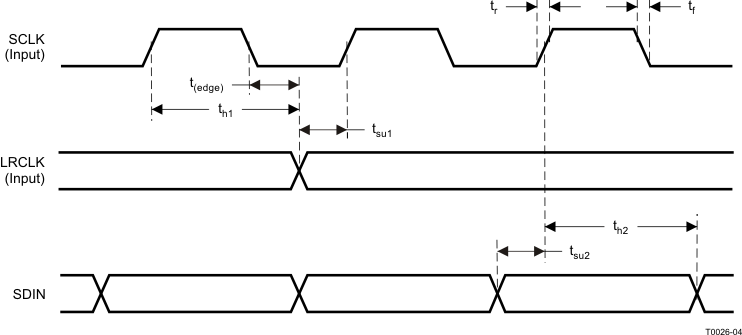 Figure 1. Slave-Mode Serial Data-Interface Timing
 Figure 2. SCL and SDA Timing
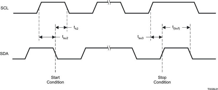 Figure 3. Start and Stop Conditions Timing

NOTES:
On power up, it is recommended that the TAS5731M RESET be held LOW for at least 100 μs after DVDD has reached 3 V.If RESET is asserted LOW while PDN is LOW, then RESET must continue to be held LOW for at least 100 μs after PDN is deasserted (HIGH).
7.14 Typical Characteristics
7.14.1 Typical Characteristics, 2.1 SE Configuration, 4 Ω
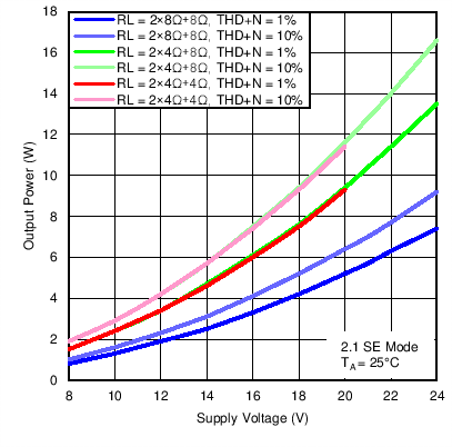 Figure 5. Output Power vs Supply Voltage (2.1 SE Mode)
 With 2 × 4ω + 4ω Load on Typical 2 Layer PCB Device May Be Thermally Limited Above 20 V
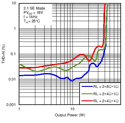 Figure 7. Total Harmonic Distortion + Noise vs Output Power (2.1 SE Mode)
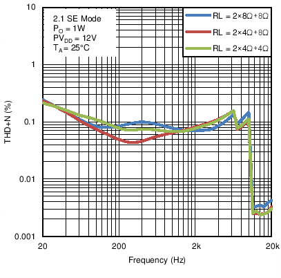 Figure 9. Total Harmonic Distortion + Noise vs Frequency (2.1 SE Mode)
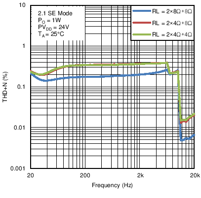 Figure 11. Total Harmonic Distortion + Noise vs Frequency (2.1 SE Mode)
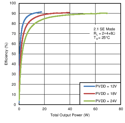 Figure 13. Efficiency vs Total Output Power (2.1 SE Mode)
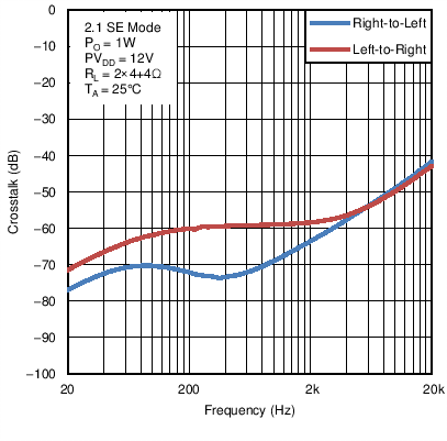 Figure 15. Crosstalk vs Frequency (2.1 SE Mode)
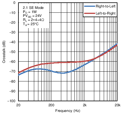 Figure 17. Crosstalk vs Frequency (2.1 SE Mode)
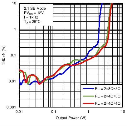 Figure 6. Total Harmonic Distortion + Noise vs Output Power (2.1 SE Mode)
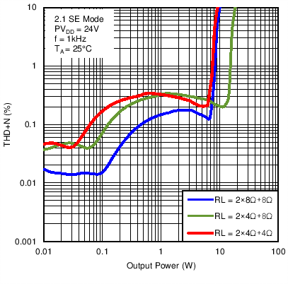 Figure 8. Total Harmonic Distortion + Noise vs Output Power (2.1 SE Mode)
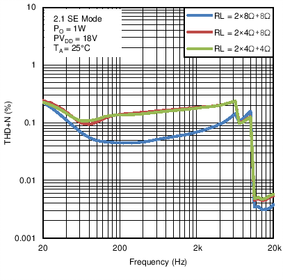 Figure 10. Total Harmonic Distortion + Noise vs Frequency (2.1 SE Mode)
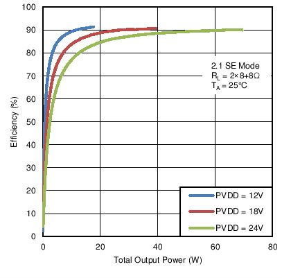 Figure 12. Efficiency vs Total Output Power (2.1 SE Mode)
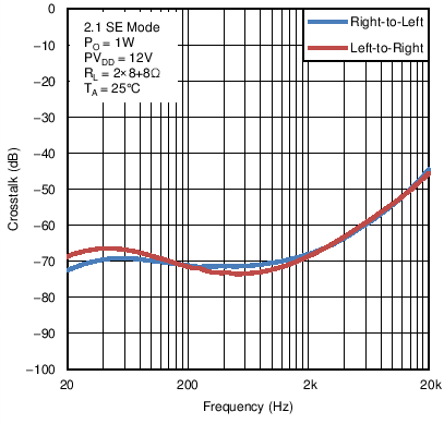 Figure 14. Crosstalk vs Frequency (2.1 SE Mode)
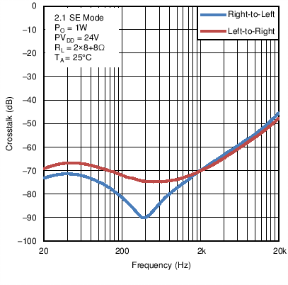 Figure 16. Crosstalk vs Frequency (2.1 SE Mode)
7.14.2 Typical Characteristics, 2.0 BTL Configuration, 8 Ω
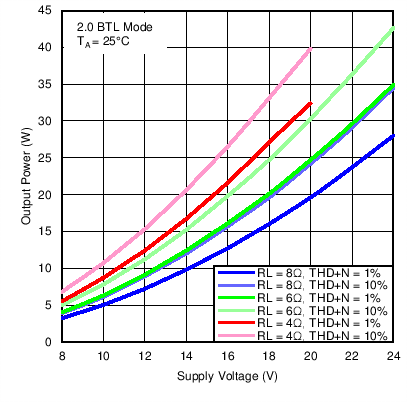 Figure 18. Output Power vs Supply Voltage (2.0 BTL Mode)
 With 4ω Load on Typical 2 Layer PCB Device May Be Thermally Limited Above 20 V
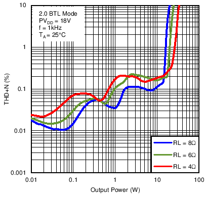 Figure 20. Total Harmonic Distortion + Noise vs Output Power (2.0 BTL Mode)
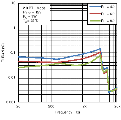 Figure 22. Total Harmonic Distortion vs Frequency (2.0 BTL Mode)
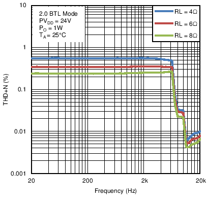 Figure 24. Total Harmonic Distortion vs Frequency (2.0 BTL Mode)
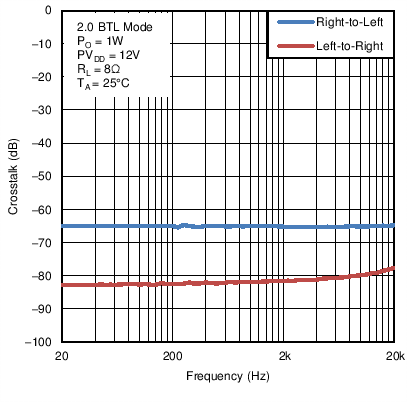 Figure 26. Crosstalk vs Frequency (2.0 BTL Mode)
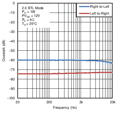 Figure 28. Crosstalk vs Frequency (2.0 BTL Mode)
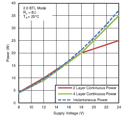 Figure 30. Power vs Supply Voltage (2.0 BTL Mode)
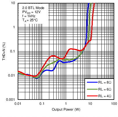 Figure 19. Total Harmonic Distortion + Noise vs Output Power (2.0 BTL Mode)
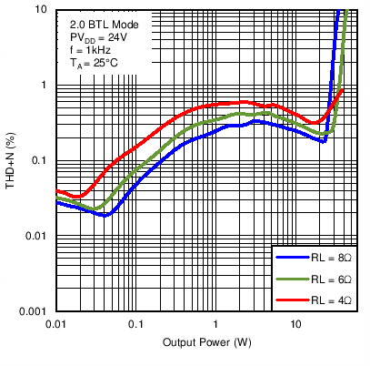 Figure 21. Total Harmonic Distortion + Noise vs Output Power (2.0 BTL Mode)
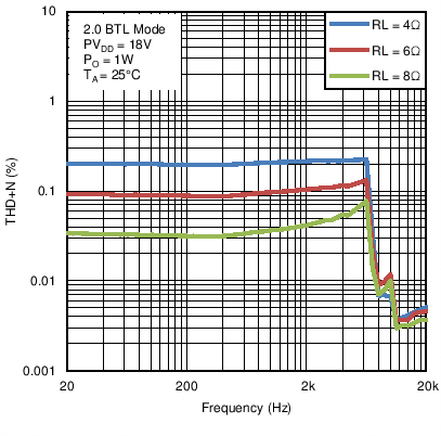 Figure 23. Total Harmonic Distortion vs Frequency (2.0 BTL Mode)
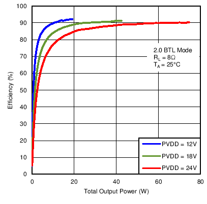 Figure 25. Efficiency vs Output Power (2.0 BTL Mode)
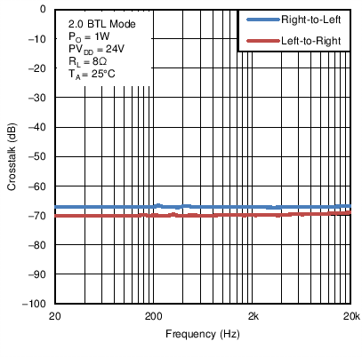 Figure 27. Crosstalk vs Frequency (2.0 BTL Mode)
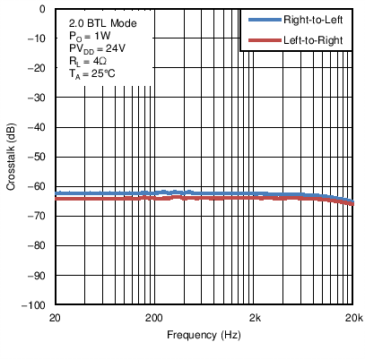 Figure 29. Crosstalk vs Frequency (2.0 BTL Mode)
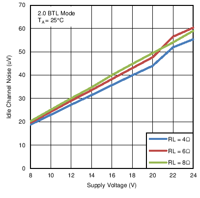 Figure 31. Idle Channel Noise vs Supply Voltage (2.0 BTL Mode)
7.14.3 Typical Characteristics, PBTL Configuration, 8 Ω
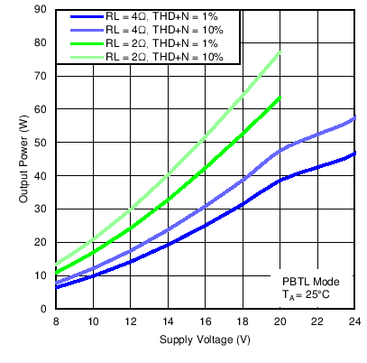 Figure 32. Output Power vs Supply Voltage (PBTL Mode)
With 2ω Load on Typical 2 Layer PCB, Device May Be Thermally Limited Above 20 V
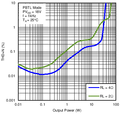 Figure 34. Total Harmonic Distortion + Noise vs Output Power (PBTL Mode)
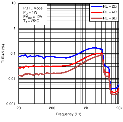 Figure 36. Total Harmonic Distortion vs Frequency (PBTL Mode)
 Figure 38. Total Harmonic Distortion vs Frequency (PBTL Mode)
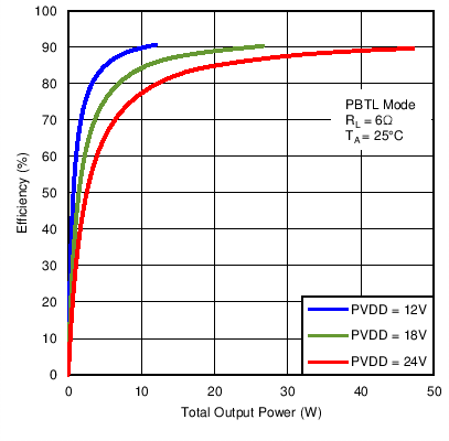 Figure 40. Efficiency vs Output Power (PBTL Mode)
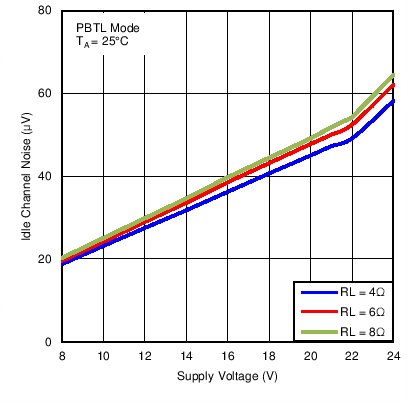 Figure 42. Idle Channel Noise vs Supply Voltage (PBTL Mode)
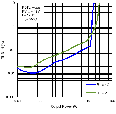 Figure 33. Total Harmonic Distortion + Noise vs Output Power (PBTL Mode)
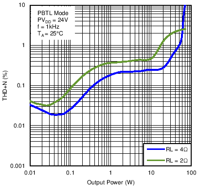 Figure 35. Total Harmonic Distortion + Noise vs Output Power (PBTL Mode)
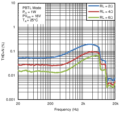 Figure 37. Total Harmonic Distortion vs Frequency (PBTL Mode)
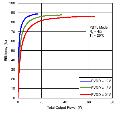 Figure 39. Efficiency vs Output Power (PBTL Mode)
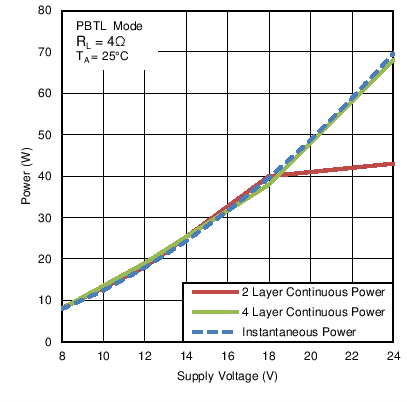 Figure 41. Power vs Supply Voltage (PBTL Mode)