ZHCSB75E May 2013 – June 2016 TAS5729MD
PRODUCTION DATA.
- 1 特性
- 2 应用
- 3 描述
- 4 修订历史记录
- 5 Related Devices
- 6 Pin Configuration and Functions
-
7 Specifications
- 7.1 Absolute Maximum Ratings
- 7.2 ESD Ratings
- 7.3 Recommended Operating Conditions
- 7.4 Thermal Information
- 7.5 Digital I/O Pins
- 7.6 Master Clock
- 7.7 Serial Audio Port
- 7.8 Protection Circuitry
- 7.9 Speaker Amplifier in All Modes
- 7.10 Speaker Amplifier in Stereo Bridge Tied Load (BTL) Mode
- 7.11 Speaker Amplifier in Stereo Post-Filter Parallel Bridge Tied Load (Post-Filter PBTL) Mode
- 7.12 Headphone Amplifier and Line Driver
- 7.13 Reset Timing
- 7.14 I2C Control Port
- 7.15 Typical Electrical Power Consumption
- 7.16 Typical Characteristics
- 8 Parameter Measurement Information
-
9 Detailed Description
- 9.1 Overview
- 9.2 Functional Block Diagram
- 9.3 Feature Description
- 9.4 Device Functional Modes
- 9.5 Programming
- 9.6
Register Maps
- 9.6.1 Clock Control Register (0x00)
- 9.6.2 Device ID Register (0x01)
- 9.6.3 Error Status Register (0x02)
- 9.6.4 System Control Register 1 (0x03)
- 9.6.5 Serial Data Interface Register (0x04)
- 9.6.6 System Control Register 2 (0x05)
- 9.6.7 Soft Mute Register (0x06)
- 9.6.8 Volume Registers (0x07, 0x08, 0x09)
- 9.6.9 Volume Configuration Register (0x0E)
- 9.6.10 Modulation Limit Register (0x10)
- 9.6.11 Interchannel Delay Registers (0x11, 0x12, 0x13, and 0x14)
- 9.6.12 PWM Shutdown Group Register (0x19)
- 9.6.13 Start/Stop Period Register (0x1A)
- 9.6.14 Oscillator Trim Register (0x1B)
- 9.6.15 BKND_ERR Register (0x1C)
- 9.6.16 Input Multiplexer Register (0x20)
- 9.6.17 Channel 4 Source Select Register (0x21)
- 9.6.18 PWM Output MUX Register (0x25)
- 9.6.19 AGL Control Register (0x46)
- 9.6.20 PWM Switching Rate Control Register (0x4F)
- 9.6.21 EQ Control (0x50)
-
10Application and Implementation
- 10.1 Application Information
- 10.2
Typical Applications
- 10.2.1 Stereo BTL Configuration With Headphone and Line Driver Amplifier
- 10.2.2 Mono PBTL Configuration with Headphone and Line Driver Amplifier
- 11Power Supply Recommendations
- 12Layout
- 13器件和文档支持
- 14机械、封装和可订购信息
10 Application and Implementation
NOTE
Information in the following applications sections is not part of the TI component specification, and TI does not warrant its accuracy or completeness. TI’s customers are responsible for determining suitability of components for their purposes. Customers should validate and test their design implementation to confirm system functionality.
10.1 Application Information
These typical connection diagrams highlight the required external components and system level connections for proper operation of the device in several popular use cases.
Each of these configurations can be realized using the Evaluation Modules (EVMs) for the device. These flexible modules allow full evaluation of the device in the most common modes of operation. Any design variation can be supported by TI through schematic and layout reviews. Visit http://e2e.ti.com for design assistance and join the audio amplifier discussion forum for additional information.
10.2 Typical Applications
These application circuits detail the recommended component selection and board configurations for the TAS5729MD device.
For further information regarding component selection, see TAS5721xx, TAS5723xx, and TAS5729xx Evaluation Module (SLOU367).
10.2.1 Stereo BTL Configuration With Headphone and Line Driver Amplifier
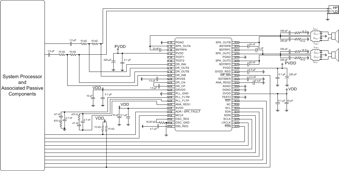
A stereo system generally refers to a system in which are two full range speakers without a separate amplifier path for the speakers that reproduce the low-frequency content. In this system, two channels are presented to the amplifier via the digital input signal. These two channels are amplified and then sent to two separate speakers.
Most commonly, the two channels are a pair of signals called a stereo pair, with one channel containing the audio for the left channel and the other channel containing the audio for the right channel.
This configuration also has a DirectPath headphone stereo amplifier which can be used independently from the speaker channels.
The Stereo BTL Configuration with Headphone and Line Driver Amplifier application is shown in Figure 55.
 Figure 55. Stereo BTL Configuration With Headphone and Line Driver Amplifier
10.2.1.1 Design Requirements
Power supplies:
- 3.3-V power supply for internal digital, analog, and headphone/line driver circuitry.
- 4.5-V to 25-V power supply for internal power circuitry
Communication:
- System controller with I2C control interface serving a compliant master
Audio digital input:
- Serial data in 16-, 20-, or 24-bit left-justified, right-justified, or I2S format
Headphone/line driver input:
- Analog single-ended line input
Output components:
- 2 × 8-Ω speakers (recommended).
- 16-Ω headphones (recommended) / 5-kΩ line driver load
Output filter:
- 4 × 15-µH Inductors
- 4 × 0.33-µF Capacitors
Components required:
- 4 × 10-kΩ Resistor
- 2 × 470-Ω Resistor
- 2 × 15-kΩ Resistor
- 1 × 18.2-kΩ Resistor
- 4 × 18-Ω Resistor
- 2 × 1.5-µF Capacitor
- 4 × 4.7-nF Capacitor
- 3 × 10-µF Capacitor
- 3 × 1-µF Capacitor
- 6 × 0.1-µF Capacitor
- 4 × 33-nF Capacitor
- 2 × 220-µF Capacitor
- 1 × 4.7-µF Capacitor
- 1 × 2.2-µF Capacitor
- 4 × 330-pF Capacitor
10.2.1.2 Detailed Design Procedure
10.2.1.2.1 Hardware Integration
- Using the Typical Application Schematic as a guide, integrate the hardware into the system schematic.
- Following the recommended component placement, schematic layout and routing given in the layout example below, integrate the device and its supporting components into the system PCB file.
- The most critical sections of the circuit are the power supply inputs, the amplifier output signals, and the high-frequency signals which go to the serial audio port. These sections should be constructed to ensure they are given precedent as design trade-offs are made.
- For questions and support go to the E2E forums (e2e.ti.com). If the user must deviate from the recommended layout, please visit the E2E forum to request a layout review.
10.2.1.2.2 Control and Software Integration
Use TAS5729 EVM and the Purepath Console GUI for device control and configuration. Prior approval is required to download the GUI. Please request access at http://www.ti.com/tool/purepathconsole.
10.2.1.2.3 Recommended Start-Up and Shutdown Procedures
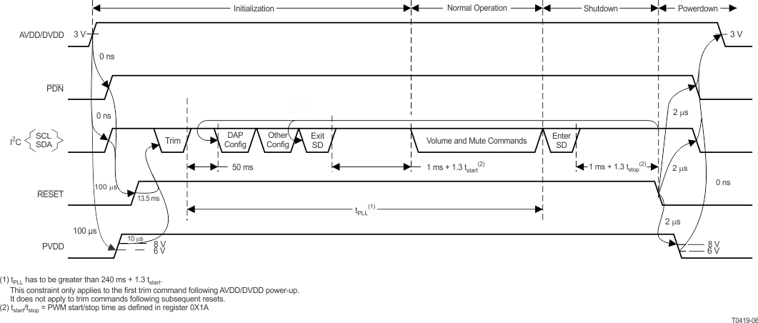
 Figure 56. Recommended Command Sequence
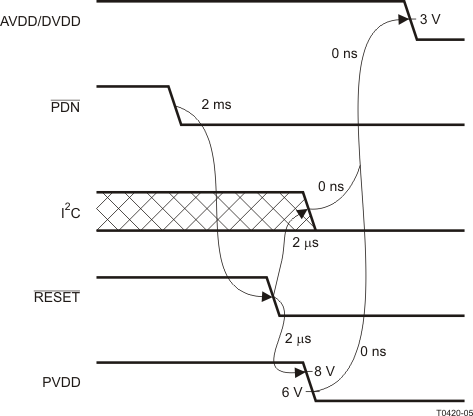
 Figure 57. Power-Loss Sequence
10.2.1.2.3.1 Initialization Sequence
Use the following sequence to power up and initialize the TAS5729MD device:
- Hold all digital inputs low and ramp up AVDD/DVDD to at least 3 V.
- Initialize digital inputs and PVDD supply as follows:
- Drive RESET = 0, PDN = 1, and other digital inputs to their desired state while ensuring that all are never more than 2.5 V above AVDD/DVDD. Wait at least 100 μs, drive RESET = 1, and wait at least another 13.5 ms.
- Ramp up PVDD to at least 8 V while ensuring that it remains below 6 V for at least 100 μs after AVDD/DVDD reaches 3 V. Then wait at least another 10 μs.
- Trim oscillator (write 0x00 to register 0x1B) and wait at least 50 ms.
- Configure the DAP via I2C, see the TAS5731EVM Evaluation Module User's Guide (SLOU331) for typical values.
- Configure remaining registers.
- Exit shutdown (sequence defined in Shutdown Sequence).
10.2.1.2.3.2 Normal Operation
The following are the only events supported during normal operation:
- Writes to master/channel volume registers
- Writes to soft-mute register
- Enter and exit shutdown (sequence defined in Shutdown Sequence)
10.2.1.2.3.3 Shutdown Sequence
Enter:
- Write 0x40 to register 0x05.
- Wait at least 1 ms + 1.3 × tstop (where tstop is specified by register 0x1A).
- If desired, reconfigure by returning to step 4 of initialization sequence.
Exit:
- Write 0x00 to register 0x05 (exit shutdown command may not be serviced for as much as 240 ms after trim following AVDD/DVDD power-up ramp).
- Wait at least 1 ms + 1.3 × tstart (where tstart is specified by register 0x1A).
- Proceed with normal operation.
10.2.1.2.3.4 Power-Down Sequence
Use the following sequence to power down the device and its supplies:
- If time permits, enter shutdown (sequence defined in Shutdown Sequence); else, in case of sudden power loss, assert PDN = 0 and wait at least 2 ms.
- Assert RESET = 0.
- Drive digital inputs low and ramp down PVDD supply as follows:
- Drive all digital inputs low after RESET has been low for at least 2 μs.
- Ramp down PVDD while ensuring that it remains above 8 V until RESET has been low for at least 2 μs.
- Ramp down AVDD/DVDD while ensuring that it remains above 3 V until PVDD is below 6 V and that it is never more than 2.5 V below the digital inputs.
10.2.1.3 Application Curves for Stereo BTL Configuration with Headphone and Line Driver Amplifier
Table 25. Stereo BTL Configuration with Headphone and Line Driver Amplifier Application Curves
| PLOT TITLE | FIGURE |
|---|---|
| Output Power vs PVDD | Figure 3 |
| THD+N vs Frequency, VPVDD = 12 V | Figure 5 |
| THD+N vs Frequency, VPVDD = 18 V | Figure 6 |
| THD+N vs Frequency, VPVDD = 24 V | Figure 7 |
| Idle Channel Noise vs PVDD | Figure 11 |
| THD+N vs Output Power, VPVDD = 12 V | Figure 13 |
| THD+N vs Output Power, VPVDD = 18 V | Figure 14 |
| THD+N vs Output Power, VPVDD = 24 V | Figure 15 |
| Efficiency vs Output Power | Figure 19 |
| Crosstalk vs Frequency, VPVDD = 12 V | Figure 21 |
| Headphone THD+N vs Frequency, VDRVDD = 3.3 V | Figure 25 |
| Headphone THD+N vs Output Power, VDRVDD = 3.3 V | Figure 26 |
| Headphone Crosstalk vs Frequency, VDRVDD = 3.3 V, RHP = 16 Ω | Figure 27 |
| Headphone Crosstalk vs Frequency, VDRVDD = 3.3 V, RHP = 32 Ω | Figure 28 |
| Line Driver THD+N vs Frequency, VDRVDD = 3.3 V | Figure 29 |
| Line Driver THD+N vs Output Voltage, VDRVDD = 3.3 V | Figure 30 |
| Line Driver Crosstalk vs Frequency, VDRVDD = 3.3 V | Figure 31 |
10.2.2 Mono PBTL Configuration with Headphone and Line Driver Amplifier
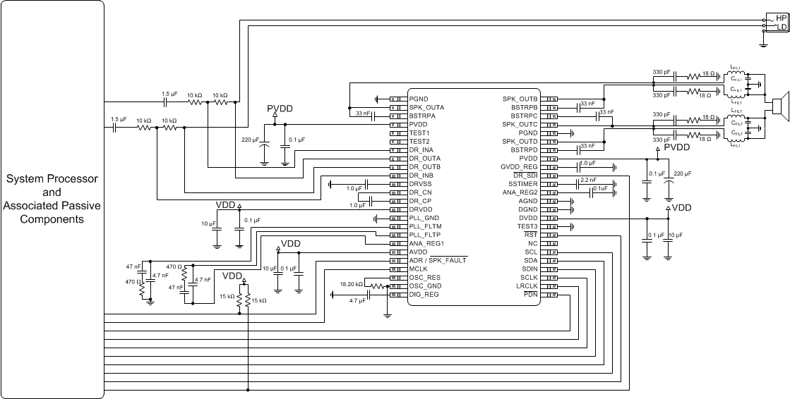
A mono system refers to a system in which the amplifier is used to drive a single loudspeaker. Parallel Bridge Tied Load (PBTL) indicates that the two full-bridge channels of the device are placed in parallel and drive the loudspeaker simultaneously using an identical audio signal. The primary benefit of operating the TAS5729MD device in PBTL operation is to reduce the power dissipation and increase the current sourcing capabilities of the amplifier output. In this mode of operation, the current limit of the audio amplifier is approximately doubled while the on-resistance is approximately halved.
The loudspeaker can be a full-range transducer or one that only reproduces the low-frequency content of an audio signal, as in the case of a powered subwoofer. Often in this use case, two stereo signals are mixed together and sent through a low-pass filter to create a single audio signal which contains the low-frequency information of the two channels.
This configuration also has a DirectPath headphone stereo amplifier which can be used independently from the speaker channel.
The Mono PBTL Configuration with Headphone and Line Driver Amplifier application is shown in Figure 58.
 Figure 58. Mono PBTL Configuration with Headphone and Line Driver Amplifier
10.2.2.1 Design Requirements
Power supplies:
- 3.3-V power supply for internal digital, analog, and headphone/line driver circuitry.
- 4.5-V to 26-V power supply for internal power circuitry
Communication:
- System controller with I2C control interface serving a compliant master
Audio digital input:
- Serial data in 16-, 20-, or 24-bit left-justified, right-justified, or I2S format
Headphone/line driver input:
- Analog single-ended line input
Output components:
- 1 × 4-Ω speaker (recommended).
- 16-Ω headphones (recommended) / 5-kΩ line driver load
Output filter:
- 4 × 15-µH Inductors
- 4 × 0.33-µF Capacitors
Components required:
- 4 × 10-kΩ Resistor
- 2 × 470-Ω Resistor
- 2 × 15-kΩ Resistor
- 1 × 18.2-kΩ Resistor
- 4 × 18-Ω Resistor
- 2 × 1.5-µF Capacitor
- 4 × 4.7-nF Capacitor
- 3 × 10-µF Capacitor
- 3 × 1-µF Capacitor
- 6 × 0.1-µF Capacitor
- 4 × 33-nF Capacitor
- 2 × 220-µF Capacitor
- 1 × 4.7-µF Capacitor
- 1 × 2.2-µF Capacitor
- 4 × 330-pF Capacitor
10.2.2.2 Detailed Design Procedure
See Stereo BTL Configuration With Headphone and Line Driver Amplifier.
10.2.2.3 Application Curves
Table 26. Mono PBTL Configuration with Headphone and Line Driver Amplifier Application Curves
| PLOT TITLE | FIGURE |
|---|---|
| Output Power vs PVDD | Figure 4 |
| THD+N vs Frequency, VPVDD = 12 V | Figure 8 |
| THD+N vs Frequency, VPVDD = 18 V | Figure 9 |
| THD+N vs Frequency, VPVDD = 24 V | Figure 10 |
| Idle Channel Noise vs PVDD | Figure 12 |
| THD+N vs Output Power, VPVDD = 12 V | Figure 16 |
| THD+N vs Output Power, VPVDD = 18 V | Figure 17 |
| THD+N vs Output Power, VPVDD = 24 V | Figure 18 |
| Efficiency vs Output Power | Figure 20 |
| Crosstalk vs Frequency, VPVDD = 12 V | Figure 22 |
| Headphone THD+N vs Frequency, VDRVDD = 3.3 V | Figure 25 |
| Headphone THD+N vs Output Power, VDRVDD = 3.3 V | Figure 26 |
| Headphone Crosstalk vs Frequency, VDRVDD = 3.3 V, RHP = 16 Ω | Figure 27 |
| Headphone Crosstalk vs Frequency, VDRVDD = 3.3 V, RHP = 32 Ω | Figure 28 |
| Line Driver THD+N vs Frequency, VDRVDD = 3.3 V | Figure 29 |
| Line Driver THD+N vs Output Voltage, VDRVDD = 3.3 V | Figure 30 |
| Line Driver Crosstalk vs Frequency, VDRVDD = 3.3 V | Figure 31 |