SLLS846C May 2009 – August 2014 SN75LVDS83B
PRODUCTION DATA.
- 1 Features
- 2 Applications
- 3 Description
- 4 Revision History
- 5 Description (Continued)
- 6 Pin Configuration and Functions
- 7 Specifications
- 8 Parameter Measurement Information
- 9 Detailed Description
- 10Application and Implementation
- 11Power Supply Recommendations
- 12Layout
- 13Device and Documentation Support
- 14Mechanical, Packaging, and Orderable Information
6 Pin Configuration and Functions
56-PIN
DGG PACKAGE
(TOP VIEW)
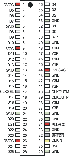
DGG Pin List
| PIN | SIGNAL | PIN | SIGNAL | PIN | SIGNAL | PIN | SIGNAL |
|---|---|---|---|---|---|---|---|
| 1 | IOVCC | 15 | D15 | 29 | GND | 43 | GND |
| 2 | D5 | 16 | D16 | 30 | D26 | 44 | LVDSVCC |
| 3 | D6 | 17 | CLKSEL | 31 | CLKIN | 45 | Y1P |
| 4 | D7 | 18 | D17 | 32 | SHTDN | 46 | Y1M |
| 5 | GND | 19 | D18 | 33 | GND | 47 | Y0P |
| 6 | D8 | 20 | D19 | 34 | PLLVCC | 48 | Y0M |
| 7 | D9 | 21 | GND | 35 | GND | 49 | GND |
| 8 | D10 | 22 | D20 | 36 | GND | 50 | D27 |
| 9 | VCC | 23 | D21 | 37 | Y3P | 51 | D0 |
| 10 | D11 | 24 | D22 | 38 | Y3M | 52 | D1 |
| 11 | D12 | 25 | D23 | 39 | CLKOUTP | 53 | GND |
| 12 | D13 | 26 | IOVCC | 40 | CLKOUTM | 54 | D2 |
| 13 | GND | 27 | D24 | 41 | Y2P | 55 | D3 |
| 14 | D14 | 28 | D25 | 42 | Y2M | 56 | D4 |
56-PIN
ZQL PACKAGE
(TOP VIEW)
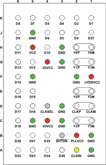
ZQL Pin List
| BALL | SIGNAL | BALL | SIGNAL | BALL | SIGNAL |
|---|---|---|---|---|---|
| A1 | GND | A2 | CLKIN | A3 | D26 |
| A4 | D24 | A5 | D23 | A6 | D22 |
| B1 | GND | B2 | PLLVCC | B3 | SHTDN |
| B4 | D25 | B5 | D21 | B6 | D20 |
| C1 | Y3M | C2 | Y3P | C3 | GND |
| C4 | IOVCC | C5 | GND | C6 | D19 |
| D1 | CLKM | D2 | CLKP | D3 | GND |
| D4 | CLKSEL | D5 | D18 | D6 | D17 |
| E1 | Y2M | E2 | Y2P | E3 | ball not populated |
| E4 | ball not populated | E5 | D15 | E6 | D16 |
| F1 | LVDSVCC | F2 | GND | F3 | ball not populated |
| F4 | ball not populated | F5 | GND | F6 | D14 |
| G1 | Y1M | G2 | Y1P | G3 | GND |
| G4 | IOVCC | G5 | D12 | G6 | D13 |
| H1 | Y0M | H2 | Y0P | H3 | GND |
| H4 | D10 | H5 | VCC | H6 | D11 |
| J1 | D27 | J2 | D0 | J3 | D3 |
| J4 | D6 | J5 | GND | J6 | D9 |
| K1 | D1 | K2 | D2 | K3 | D4 |
| K4 | D5 | K5 | D7 | K6 | D8 |
Pin Functions
| PIN | I/O | DESCRIPTION |
|---|---|---|
| Y0P, Y0M, Y1P, Y1M, Y2P, Y2M | LVDS Out | Differential LVDS data outputs. Outputs are high-impedance when SHTDN is pulled low (de-asserted) |
| Y3P, Y3M | Differential LVDS Data outputs. Output is high-impedance when SHTDN is pulled low (de-asserted). Note: if the application only requires 18-bit color, this output can be left open. |
|
| CLKP, CLKM | Differential LVDS pixel clock output. Output is high-impedance when SHTDN is pulled low (de-asserted). |
|
| D0 – D27 | CMOS IN with pulldn | Data inputs; supports 1.8 V to 3.3 V input voltage selectable by VDD supply. To connect a graphic source successfully to a display, the bit assignment of D[27:0] is critical (and not necessarily intuitive). For input bit assignment see Figure 15 to Figure 18 for details. Note: if application only requires 18-bit color, connect unused inputs D5, D10, D11, D16, D17, D23, and D27 to GND. |
| CLKIN | Input pixel clock; rising or falling clock polarity is selectable by Control input CLKSEL. | |
| SHTDN | Device shut down; pull low (de-assert) to shut down the device (low power, resets all registers) and high (assert) for normal operation. | |
| CLKSEL | Selects between rising edge input clock trigger (CLKSEL = VIH) and falling edge input clock trigger (CLKSEL = VIL). | |
| VCC | Power Supply(1) | 3.3 V digital supply voltage |
| IOVCC | I/O supply reference voltage (1.8 V up to 3.3 V matching the GPU data output signal swing) | |
| PLLVCC | 3.3 V PLL analog supply | |
| LVDSVCC | 3.3 V LVDS output analog supply | |
| GND | Supply ground for VCC, IOVCC, LVDSVCC, and PLLVCC. |
(1) For a multilayer pcb, it is recommended to keep one common GND layer underneath the device and connect all ground terminals directly to this plane.