SLLS980E June 2009 – November 2016 SN75LVDS83A
PRODUCTION DATA.
- 1 Features
- 2 Applications
- 3 Description
- 4 Revision History
- 5 Description (continued)
- 6 Pin Configuration and Functions
- 7 Specifications
- 8 Parameter Measurement Information
- 9 Detailed Description
- 10Application and Implementation
- 11Power Supply Recommendations
- 12Layout
- 13Device and Documentation Support
- 14Mechanical, Packaging, and Orderable Information
1 Features
- LVDS Display SerDes Interfaces Directly to LCD Display Panels with Integrated LVDS
- Package Options: 8.1 mm × 14 mm TSSOP
- 3.3-V Tolerant Data Inputs
- Transfer Rate up to 100 Mpps (Mega Pixel Per Second)
- Pixel Clock Frequency Range: 10 MHz to 100 MHz
- Suited for Display Resolutions Ranging From HVGA up to HD With Low EMI
- Operates From a Single 3.3-V Supply and
170 mW (Typical) at 75 MHz - 28 Data Channels Plus Clock In Low-Voltage TTL to 4 Data Channels Plus Clock Out Low-Voltage Differential
- Consumes Less Than 1 mW When Disabled
- Selectable Rising or Falling Clock Edge Triggered Inputs
- ESD: 5000 V HBM
- Support Spread Spectrum Clocking (SSC)
- Compatible With all OMAP™ 2x, OMAP™ 3x, and DaVinci™ Application Processors
2 Applications
- Tablets
- Industrial PC, Laptop, and Other Factory Automation Displays
- Patient Monitor and Medical Equipment Displays
- Electronic Point-of-Sale (EPOS) Displays
- Printer Displays
3 Description
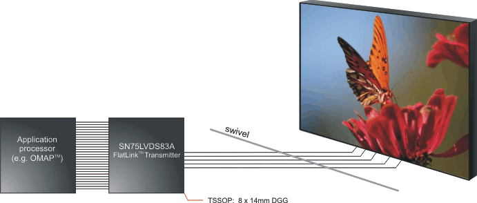
The SN75LVDS83A Flatlink™ transmitter device contains four 7-bit parallel-load serial-out shift registers, a 7× clock synthesizer, and five Low-Voltage Differential Signaling (LVDS) line drivers in a single integrated circuit. These functions allow 28 bits of single-ended LVTTL data to be synchronously transmitted over five balanced-pair conductors for receipt by a compatible receiver, such as the SN75LVDS82 and LCD panels with integrated LVDS receiver.
When transmitting, data bits D0 through D27 are each loaded into registers upon the edge of the input clock signal (CLKIN). The rising or falling edge of the clock can be selected via the clock select (CLKSEL) pin. The frequency of CLKIN is multiplied seven times, and then used to unload the data registers in 7-bit slices and serially. The four serial streams and a phase-locked clock (CLKOUT) are then output to LVDS output drivers. The frequency of CLKOUT is the same as the input clock, CLKIN.
Device Information(1)
| PART NUMBER | PACKAGE | BODY SIZE (NOM) |
|---|---|---|
| SN75LVDS83A | TSSOP (56) | 14.00 mm × 6.10 mm |
- For all available packages, see the orderable addendum at the end of the data sheet.
LVDS Application
