ZHCSEG3C September 2015 – July 2016 SN65DP149 , SN75DP149
PRODUCTION DATA.
- 1 特性
- 2 应用
- 3 说明
- 4 修订历史记录
- 5 说明 (续)
- 6 Pin Configuration and Functions
-
7 Specifications
- 7.1 Absolute Maximum Ratings
- 7.2 ESD Ratings
- 7.3 Recommended Operating Conditions
- 7.4 Thermal Information
- 7.5 Power Supply Electrical Characteristics
- 7.6 Differential Input Electrical Characteristics
- 7.7 HDMI and DVI TMDS Output Electrical Characteristics
- 7.8 DDC, and I2C Electrical Characteristics
- 7.9 HPD Electrical Characteristics
- 7.10 HDMI and DVI Main Link Switching Characteristics
- 7.11 HPD Switching Characteristics
- 7.12 DDC and I2C Switching Characteristics
- 7.13 Typical Characteristics
- 8 Parameter Measurement Information
- 9 Detailed Description
- 10Application and Implementation
- 11Power Supply Recommendations
- 12Layout
- 13器件和文档支持
- 14机械、封装和可订购信息
9 Detailed Description
9.1 Overview
The SNx5DP149 device is a Dual Mode[1] DisplayPort retiming level shifter that supports data rates up to 3.4-Gbps for HDMI1.4b. The device takes in AC coupled HDMI/DVI signals and level shifts them to TMDS signals while compensating for loss and jitter through its receiver equalizer and retiming functions. The SNx5DP149 in default configuration should meet most system needs but also provides features that allow the system implementer flexibility in design. Programming can be accomplished through I2C[4] or pin strapping.
9.2 Functional Block Diagram
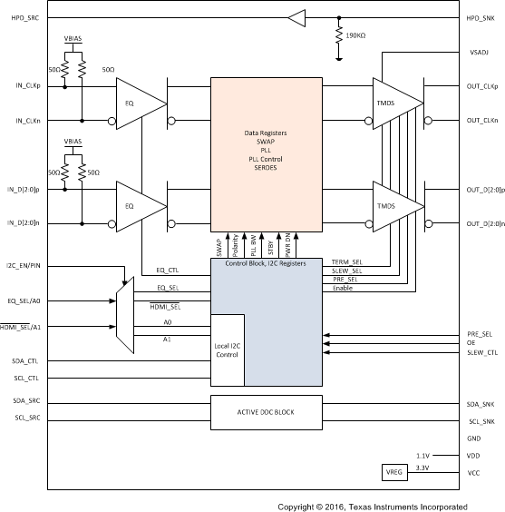
9.3 Feature Description
9.3.1 Reset Implementation
When OE is de-asserted, control signal inputs are ignored; the Dual Mode[1] DisplayPort inputs and outputs are high impedance. It is critical to transition the OE input from a low level to a high level after the VCC supply has reached the minimum recommended operating voltage. Achieve this transition by a control signal to the OE input, or by an external capacitor connected between OE and GND. To ensure that the SNx5DP149 device is properly reset, the OE pin must be de-asserted for at least 100-μs before being asserted. When OE is toggled in this manner the device is reset. This requires the device to be reprogrammed if it was originally programmed through I2C for configuration. When implementing the external capacitor, the size of the external capacitor depends on the power-up ramp of the VCC supply, where a slower ramp-up results in a larger value external capacitor. Refer to the latest reference schematic for SNx5DP149; consider approximately 200-nF capacitor as a reasonable first estimate for the size of the external capacitor. Both OE implementations are shown in Figure 19 and Figure 20.
SPACE
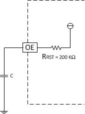 Figure 19. External Capacitor Controlled OE
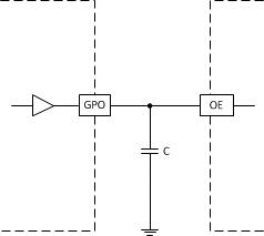 Figure 20. OE Input from Active Controller
9.3.2 Operation Timing
SNx5DP149 starts to operate after the OE signal goes high (see Figure 21, Figure 22, and Table 1). Keeping OE low until VDD and VCC become stable avoids any timing requirements as shown in Figure 21.
 Figure 22. CDR Timing for SNx5DP149
Table 1. SNx5DP149 Operation Timing
9.3.3 Input Lane Swap and Polarity Working
The SNx5DP149 device incorporates the swap function, which can set the input lanes in swap mode. The IN_D2 routes to the OUT_CLK position. The IN_D1 swaps with IN_D0. The swap function only changes the input pins; EQ setup follows new mapping. The user needs to control the register 0x09h bit 7 for SWAP enable. Lane swap is operational in both redriver and retimer mode.
Table 2. Lane Swap(1)
| NORMAL OPERATION | SWAP = L OR CSR 0x09h BIT 7 IS 1’b1 |
|---|---|
| IN_D2 → OUT_D2 | IN_D2 → OUT_CLK |
| IN_D1 → OUT_D1 | IN_D1 → OUT_D0 |
| IN_D0 → OUT_D0 | IN_D2 → OUT_D1 |
| IN_CLK → OUT_CLK | IN_CLK → OUT_D2 |
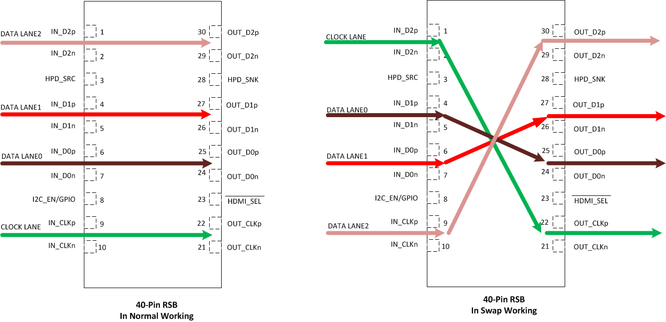 Figure 23. SNx5DP149 Swap Function for 40 Pins
The SNx5DP149 can also change the polarity of the input signals. Use Register 0x9h bit 6 to swap polarity using I2C. Polarity swap only works for retimer mode. When the device is in automatic redriver to retimer mode this only works when device is in retimer stage. If set and data rate falls below 1.0-Gbps in this mode the polarity function will be lost.
9.3.4 Main Link Inputs
Standard Dual Mode[1] DisplayPort terminations are integrated on all inputs with expected AC coupling capacitors on board prior to input pins. External terminations are not required. Each input data channel contains an adaptive or fixed equalizer to compensate for cable or board losses. The voltage at the input pins must be limited below the absolute maximum ratings. The input pins have incorporated failsafe circuits. The input pins can be polarity changed through the local I2C register.
9.3.5 Main Link Inputs Debug Tools
There are two methods for debugging a system making sure the inputs to the SNx5DP149 are valid. A TMDS error checker is implemented that will increment an error counter per data lane. This allows the system implementer to determine how the link between the source and SNx5DP149 is performing on all three data lanes. See CSR Bit Field Definitions – RX PATTERN VERIFIER CONTROL/STATUS register in Table 10.
If a high error count is evident, the SNx5DP149 has the ability to provide the general eye quality. A tool is available that uses the I2C[4] link to download data that can be plotted for an eye diagram. This is available per data lane.
9.3.6 Receiver Equalizer
Equalizers are used to clean up inter-symbol interference (ISI) jitter or loss from the bandwidth-limited board traces or cables. The SNx5DP149 device supports both fixed receiver equalizer (redriver and retimer mode) and adaptive receive equalizer (retimer mode) by setting the EQ_SEL/A0 pin or through I2C using reg0Ah[5]. When the EQ_SEL/A0 pin is high, the EQ gain is fixed to 14-dB. The EQ gain will be 7.5-dB if the EQ_SEL/A0 pin is set low. The SNx5DP149 device operates in adaptive equalizer mode when EQ_SEL/A0 left floating. Using adaptive equalization the gain will be automatically adjusted based on the data rate to compensate for variable trace or cable loss. Using the local I2C[4] control, reg0Dh[5:1], the fixed EQ gain can be selected for both data and clock.
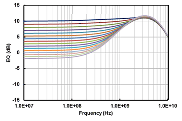 Figure 24. Adaptive EQ Gain Curve
9.3.7 Termination Impedance Control
For HDMI1.4b[2] when data rate over 2 Gbps, the output performance could be better if the termination value between 150 to 300-Ω which was allowed. For compliance this may not be the best solution so be prepared to utilize no termination. The SNx5DP149 supports two different source termination impedances for HDMI1.4b[2] . This can be adjusted by I2C[4]; reg0Bh[4:3] TX_TERM_CTL.
9.3.8 TMDS Outputs
An 1% precision resistor, 6.5-kΩ, is recommended to be connected from Vsadj pin to ground to allow the differential output swing to comply with TMDS signal levels. The differential output driver provides a typical 10-mA current sink capability when no source term is enabled, which provides a typical 500-mV voltage drop across a 50-Ω termination resistor. As compliance testing is system dependant this resistor value can be adjusted.
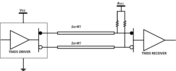 Figure 25. TMDS Driver and Termination Circuit
Referring to Figure 25, if both VCC (device supply) and AVCC (sink termination supply) are powered, the TMDS output signals are high impedance when OE = low. The normal operating condition is that both supplies are active. A total of 33-mW of power is consumed by the terminations independent of the OE logical selection. When AVCC is powered on, normal operation (OE controls output impedance) is resumed. When the power source of the device is off and the power source to termination is on, the IO(off) (output leakage current) specification ensures the leakage current is limited 45-μA or less.
The clock and data lanes VOD can be changed through I2C[4] (see VSWING_CLK and VSWING_DATA in Table 8 for details). shows the different output voltage based on different Vsadj resistor values.
9.3.8.1 Pre-Emphasis/De-Emphasis
The SNx5DP149 provides De-emphasis as a way to compensate for the ISI loss between the TMDS outputs and the receiver it is driving. There are two methods to implement this function. When in pin strapping mode the PRE_SEL pin controls this. The PRE_SEL pin provides –2-dB, or 0-dB de-emphasis, which allows output signal pre-conditioning to offset interconnect losses from the SNx5DP149 device outputs to a TMDS receiver. TI recommends setting PRE_SEL at 0 dB while connecting to a receiver through a short PCB route. When pulled to ground with a 65-kΩ resistor –2-dB can be realized, see Figure 9. When using I2C, Reg0Ch[1:0] is used to make these adjustments.
As there are times true pre-emphasis may be the best solution there are two ways to accomplish this. If pin strapping is being use the best method is to reduce the Vsadj resistor value increasing the VOD and then pulling the PRE_SEL pin to ground using the 65-kΩ resistor, see Figure 26. If using I2C this can be accomplished using two methods. First is similar to pin strapping by adjusting the Vsadj resistor value and then implementing –2-dB de-emphasis. Second method is to set Reg0Ch[7:5] = 011 and the set Reg0Ch[1:0] = 01 which accomplishes the same pre-emphasis setting. See Figure 27.
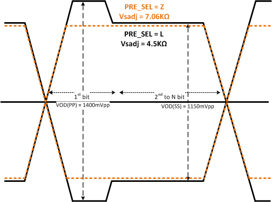 Figure 26. Pre-Emphasis Using Pin Strapping Method
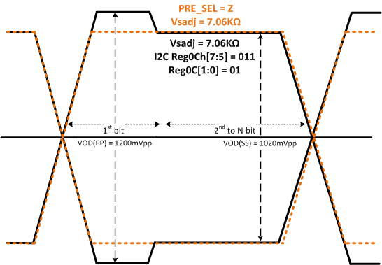 Figure 27. Pre-Emphasis Using I2C Method
9.4 Device Functional Modes
9.4.1 Retimer Mode
Clock and data recovery circuits (CDR) are used to track, sample and retime the equalized data bit streams. The CDRs are designed with loop bandwidth to minimize the amount of jitter transfer from the video source to the TMDS outputs. Input jitter within the CDR’s PLL bandwidth, < 1-MHz, will be transferred to the TMDS outputs. Higher frequency jitter above the CDR loop bandwidth is attenuated, providing a jitter cleaning function to reduce the amount of high frequency jitter from the video source. The retimer is automatically activated at pixel clock above approximately 100-MHz when jitter cleaning is needed for robust operation. The retimer operates at about 1.0 to 3.4-Gbps DR supporting HDMI1.4b[3]. At pixel clock frequency below about 100 MHz, the SNx5DP149 automatically bypasses the internal retimer and operates as a redriver. When the video source changes resolution, the internal retimer starts the acquisition process to determine the input clock frequency and acquire lock to the new data bit streams. During the clock frequency detection period and the retimer acquisition period (that last approximately 7-ms), the TMDS drivers can be kept active (default) or programmed to be disabled to avoid sending invalid clock or data to the downstream receiver.
9.4.2 Redriver Mode
The SNx5DP149 also has a redriver mode that can be enabled through I2C[4]; at offset address 0Ah bits 1:0 DEV_FUNC_MODE. When in this mode, the CDR and PLL are shut off, thus reducing power. Jitter performance is degraded as the device will now only compensate for ISI loss in the link. In redriver mode HDMI1.4b[3] compliance is not guaranteed as skew compensation and retiming functions are disabled. Excessive random or phase jitter will not be compensated.
9.4.3 DDC Functional Description
The SNx5DP149 solves sink- or source-level issues by implementing a master/slave control mode for the DDC bus. When the SNx5DP149 detects the start condition on the DDC bus from the SDA_SRC/SCL_SRC, it will transfer the data or clock signal to the SDA_SNK/SCL_SNK with little propagation delay. When SDA_SNK detects the feedback from the downstream device, the SNx5DP149 will pull up or pull down the SDA_SRC bus and deliver the signal to the source.
The DDC link defaults to 100 kbps, but can be set to various values including 400 kbps by setting the correct value to address 22h (see Table 3) through the I2C access on the DDC interface. The DDC lines are 5-V tolerant. The HPD_SRC goes to high impedance when VCC is under low power conditions, < 1.5-V.
9.5 Register Maps
9.5.1 DP-HDMI Adaptor ID Buffer
The SNx5DP149 device includes the DP-HDMI adapter ID buffer for HDMI/DVI adaptor recognition, defined by the VESA DisplayPort Dual-Mode Standard Version 1.1, accessible by standard I2C[4] protocols through the DDC interface when the HDMI_SEL/A1 pin is low. The DP-HDMI adapter buffer and extended DDC register for Type 2 capability is accessed at target addresses 80h (Write) and 81h (Read).
The DP-HDMI adapter buffer contains a read-only phrase DP-HDMI ADAPTOR<EOT> converted to ASCII characters, as shown in Table 3, and supports the WRITE command procedures (accessed at target address 80h) to select the subaddress, as recommended in the VESA DisplayPort Interoperability Guideline Adaptor Checklist Version 1.0 section 2.3.
Table 3. SNx5DP149 DP-HDMI Adaptor ID Buffer and Extended DDC
| Address | Description | Value HDMI | Value DVI | Read or Read/Write |
|---|---|---|---|---|
| 00h | HDMI ID code | 44h | 00h | Read only |
| 01h | 50h | 00h | ||
| 02h | 2Dh | 00h | ||
| 03h | 48h | 00h | ||
| 04h | 44h | 00h | ||
| 05h | 4Dh | 00h | ||
| 06h | 49h | 00h | ||
| 07h | 20h | 00h | ||
| 08h | 41h | 00h | ||
| 09h | 44h | 00h | ||
| 0Ah | 41h | 00h | ||
| 0Bh | 50h | 00h | ||
| 0Ch | 54h | 00h | ||
| 0Dh | 4Fh | 00h | ||
| 0Eh | 52h | 00h | ||
| 0Fh | 04h | 00h | ||
| 10h | Video Adaptor Identifier Bit 2:0 ADAPTOR_REVISION |
0 | 0 | Read only |
| Bit 3 Reserved: but 0 for type 2 | 0 | 0 | ||
| Bits 7:4 1010 = Dual mode defined by dual mode[1] standard | 1010 | 0 | ||
| 11h | IEE_OUI first two hex digits | 08h | 08h | Read only |
| 12h | IEE_OUI second two hex digits | 00h | 00h | Read only |
| 13h | IEE_OUI third two hex digits | 28h | 28h | Read only |
| 14h | Device ID | 44h | 44h | Read only |
| 15h | 50h | 50h | ||
| 16h | 31h | 31h | ||
| 17h | 34h | 34h | ||
| 18h | 39h | 39h | ||
| 19h | 00h | 00h | ||
| 1Ah | Hardware revision | 02h | 02h | Read only |
| Bits 7:4 major revision | 00h | 00h | ||
| Bits 3:0 minor revision | 02h | 02h | ||
| 1Bh | Firmware or software major revision | 00h | 00h | Read only |
| 1Ch | Firmware or software minor revision | 00h | 00h | Read only |
| 1Dh | Max TMDS clock rate Default value is 88h in HDMI column Note: Value determined by taking clock rate and dividing by 2.5 and converting to HEX. For HDMI2.0 extend as if the clock rate extended instead of its actual method, clock 1/10 DR and not 1/40 DR. |
88h | 42h | Read only |
| 1Eh | If I2C_DR_CTL = 0 the value is 0Fh → If DDC_AUX_DR_SEL = 0 the value is 0Fh If I2C_DR_CTL = 1 the value is 1Fh → If DDC_AUX_DR_SEL = 1 then value is 1Fh If I2C_DR_CTL = 0 the value is 0Fh If I2C_DR_CTL = 1 the value is 1Fh |
0Fh | 0Fh | Read only |
| 1Fh | Reserved | 00h | 00h | Write/Read |
| 20h | TMDS_OE
Bit 0: 0 = TMDS_ENABLED (default) Bit 0: 1 = TMDS_DISABLED Bits 7:1 Reserved |
00h | 00h | Write/Read |
| 21h | HDMI Pin Control Bit 0 = CEC_EN Enables connection between the HDMI CEC pin connected to the sink and the CONFIG2 pin to the upstream device + 27-kΩ pullup. 0 = CEC_ DISABLED (default) 1 = CEC_ ENABLED Bits 7:1 = RESERVED |
00h | 00h | Write/Read |
| 22h | Writing a bit pattern to this register that is not defined above may result in an unpredictable I2C speed selection, but the adaptor must continue to otherwise work normally. Only applicable when using I2C-over-AUX transport 01h = 1-Kbps 02h = 5-Kbps 04h = 10-Kbps 08h = 100-kbps 10h = 400-Kbps (RSVD in Dual Mode STND) On read, the dual-mode cable adaptor returns a value to indicate the speed currently in use. The default I2C speed prior to software writing to this register is 100-Kbps. Illegal write value shall write register default (08h). This register sets the DDC output DR whether I2C-over-AUX or straight DDC |
08h | 08h | Write/Read |
| 23h-FFh | Reserved | 00h | 00h | Read |
9.5.2 Local I2C Interface Overview
The SCL_CTL and SDA_CTL pins are used for I2C clock and I2C data respectively. The SNx5DP149 I2C interface conforms to the 2-wire serial interface defined by the I2C Bus Specification, Version 2.1 (January 2000), and supports the fast mode transfer up to 400 kbps.
The device address byte is the first byte received following the start condition from the master device. The 7-bit device address for the SNx5DP149 device decides by the combination of EQ_SEL/A0 and HDMI_SEL/A1. Table 4 clarifies the SNx5DP149 device target address.
Table 4. I2C Device Address Description
| A1/A0 | SNx5DP149 I2C Device Address | ADD | |||||||
|---|---|---|---|---|---|---|---|---|---|
| 7 (MSB) | 6 | 5 | 4 | 3 | 2 | 1 | 0 (W/R) | ||
| 00 | 1 | 0 | 1 | 1 | 1 | 1 | 0 | 0/1 | BC/BD |
| 01 | 1 | 0 | 1 | 1 | 1 | 0 | 1 | 0/1 | BA/BB |
| 10 | 1 | 0 | 1 | 1 | 1 | 0 | 0 | 0/1 | B8/B9 |
| 11 | 1 | 0 | 1 | 1 | 0 | 1 | 1 | 0/1 | B6/B7 |
9.5.3 I2C Control Behavior
Follow this procedure to write to the SNx5DP149 device I2C registers:
- The master initiates a write operation by generating a start condition (S), followed by the SNx5DP149 device 7-bit address and a zero-value W/R bit to indicate a write cycle.
- The SNx5DP149 device acknowledges the address cycle by combination of A0 and A1.
- The master presents the subaddress (I2C register within SNx5DP149 device) to be written, consisting of one byte of data, MSB-first.
- The SNx5DP149 device acknowledges the subaddress cycle.
- The master presents the first byte of data to be written to the I2C register.
- The SNx5DP149 device acknowledges the byte transfer.
- The master may continue presenting additional bytes of data to be written, with each byte transfer completing with an acknowledge from the SNx5DP149.
- The master terminates the write operation by generating a stop condition (P).
Follow this procedure to read the SNx5DP149 I2C registers:
- The master initiates a write operation by generating a start condition (S), followed by the SNx5DP149 7-bit address and a zero-value W/R bit to indicate a write cycle.
- The SNx5DP149 device acknowledges the address cycle by combination of A0 and A1.
- The master presents the subaddress (I2C register within SNx5DP159 device) to be read, consisting of one byte of data, MSB-first.
- The SNx5DP149 device acknowledges the subaddress cycle.
- The master initiates a read operation by generating a start condition (S), followed by the SNx5DP149 7-bit address and a one-value W/R bit to indicate a read cycle.
- The SNx5DP159 device acknowledges the address cycle.
- The SNx5DP149 device transmit the contents of the memory registers MSB-first starting at the written subaddress.
- The SNx5DP149 device will wait for either an acknowledge (ACK) or a not-acknowledge (NACK) from the master after each byte transfer; the I2C master acknowledges reception of each data byte transfer.
- If an ACK is received, the SNx5DP149 device transmits the next byte of data.
- The master terminates the read operation by generating a stop condition (P).
NOTE
No sub-addressing is included for the read procedure, and reads start at register offset 00h and continue byte by byte through the registers until the I2C master terminates the read operation.
Refer to Table 6 for the SNx5DP149 device local I2C register descriptions. Reads from reserved fields return 0s and writes are ignored.
9.5.4 I2C Control and Status Registers
Reads from reserved fields return 0, and writes to read-only reserved registers are ignored. Writes to reserved registers, which are marked with ‘W’, produce unexpected behavior. All addresses not defined by this specification are considered reserved. Reads from these addresses return 0 and writes will be ignored.
9.5.4.1 Bit Access Tag Conventions
A table of bit descriptions is typically included for each register description that indicates the bit field name, field description, and the field access tags. The field access tags are described in Table 5.
Table 5. Field Access Tags
| ACCESS TAG | NAME | DESCRIPTION |
|---|---|---|
| R | Read | The field is read by software |
| W | Write | The field is written by software |
| S | Set | The field is set by a write of one. Writes of 0 to the field have no effect |
| C | Clear | The field is cleared by a write of 1. Writes of 0 to the field have no effect |
| U | Update | Hardware may autonomously update this field |
| NA | No access | Not accessible or not applicable |
9.5.4.2 CSR Bit Field Definitions
9.5.4.2.1 ID Registers
Table 6. ID Registers
| ADDRESS | BIT | DESCRIPTION | ACCESS |
|---|---|---|---|
| 00h:07h | 7:0 | DEVICE_ID These fields return a string of ASCII characters “DP149” followed by three space characters. Address 0x00 – 0x07 = {0x44”D”, 0x50”P”, 0x31”1”, 0x34”4”, 0x39”9”, 0x20, 0x20, 0x20} |
R |
| 08h | 7:0 | REV _ID. This field identifies the device revision. 0000001 – DP149 revision 1 |
R |
9.5.4.2.2 Misc Control
Table 7. Misc Control
Mode Selection Definition: This bit lets the receiver know where the device is located in a system for the purpose of centering the AEQ point. The SNx5DP149 is targeting the source application, so the default value is 0, which will center the EQ at 6.5 to 7.5-dB , see Table 9. If the SNx5DP149 is in a dock or sink application, the value should be changed to a value of 1, which will center the EQ at 12 to 13-dB .
9.5.4.2.3 HDMI Control
Table 8. HDMI Control
| ADDRESS | BIT | DEFAULT | DESCRIPTION | ACCESS |
|---|---|---|---|---|
| 0Bh | 7:6 | 2’b00 | SLEW_CTL. Slew rate control.2’00 is fastest and 2’b11 is slowest Writes ignored when I2C_EN/PIN = 0 |
RWU |
| 5 | 1’b0 | HDMI_SEL: Contro; Writes ignored when I2C_EN/PIN = 0l 0 – HDMI (default) 1 – DVI |
RWU | |
| 4:3 | 2’b00 | TX_TERM_CTL: Controls termination for HDMI TX 00 – No termination 01 – 150 to 300-Ω 10 – Reserved 11 - Reserved |
RWU | |
| 2 | 1’b0 | Reserved | R | |
| 1 | 1’b0 | . Reserved
|
R | |
| 0 | 1’b0 | Reserved
|
R | |
| 0Ch | 7:5 | 3’b000 | VSWING_DATA: Data output swing control 000 – Vsadj set 001 – Increase by 7% 010 – Increase by 14% 011 – Increase by 21% 100 – Decrease by 30% 101 – Decrease by 21% 110 – Decrease by 14% 111 – Decrease by 7% |
RW |
| 4:2 | 3’b000 | VSWING_CLK: Clock Output Swing Control 000 – Vsadj set 001 – Increase by 7% 010 – Increase by 14% 011 – Increase by 21% 100 – Decrease by 30% 101 – Decrease by 21% 110 – Decrease by 14% 111 – Decrease by 7% Note: Default is set by DR, which means standard based swing values but this allows for the swing to be overridden by selecting one of these values |
RW | |
| 1:0 | 2’b00 | HDMI_TWPST1. HDMI de-emphasis FIR post-cursor-1 signed tap weight. 00 – No de-emphasis 01 – 2-dB de-emphasis 10 – Reserved 11 – Reserved |
RWU |
9.5.4.2.4 Equalization Control Register
Table 9. Equalization Control Register
| ADDRESS | BIT | DEFAULT | DESCRIPTION | ACCESS | |
|---|---|---|---|---|---|
| 0Dh | 7:6 | 2’b00 | Reserved | RW | |
| 5:3 | 1’b000 | Data Lane EQ – Sets fixed EQ values | RW | ||
| HDMI1.4b[2]
000 – 0-dB 001 – 4.5-dB 010 – 6.5-dB 011 – 8.5-dB 100 – 10.5-dB 101 – 12-dB 110 – 14-dB 111 – 16.5-dB |
|||||
| 2:1 | 1’b00 | Clock Lane EQ - Sets fixed EQ values | RW | ||
| HDMI1.4b[2]
00 – 0-dB 01 – 1.5-dB 10 – 3-dB 11 – RSVD |
|||||
| 0 | 1’b0 | Reserved
|
RW | ||
9.5.4.2.5 EyeScan Control Register
Table 10. EyeScan Control Register
| ADDRESS | BITS | DEFAULT | DESCRIPTION | ACCESS |
|---|---|---|---|---|
| 0Eh | 7:4 | 4’b0000 | PV_SYNC[3:0]. Pattern timing pulse. This field is updated for 8UI once every cycle of the PRBS generator. 1 bit per lane. | R |
| 3:0 | 4’b0000 | PV_LD[3:0]. Load pattern-verifier controls into RX lanes. When asserted high, the PV_TO, PV_SEL, PV_LEN, PV_CP20, and PV_CP values are enabled into the corresponding RX lane. These values are then latched and held when PV_LD[n] is subsequently de-asserted low. 1 bit per lane. | RWU | |
| 0Fh | 7:4 | 4’b0000 | PV_FAIL[3:0]. Pattern verification mismatch detected. 1 bit per lane. | RU |
| 3:0 | 4’b0000 | PV_TIP[3:0]. Pattern search/training in progress. 1 bit per lane. | RU | |
| 10h | 7 | 1’b0 | PV_CP20. Customer pattern length 20 or 16 bits. 0 – 16 bits 1 – 20 bits |
RW |
| 6 | 1’b0 | Reserved | R | |
| 5:3 | 3’b000 | PV_LEN[2:0]. PRBS pattern length 000 – PRBS7 001 – PRBS11 010 – PRBS23 011 – PRBS31 100 – PRBS15 101 – PRBS15 110 – PRBS20 111 – PRBS20 |
RW | |
| 2:0 | 3’b000 | PV_SEL[24:0]. Pattern select control 000 – Disabled 001 – PRBS 010 – Clock 011 – Custom 1xx – Timing only mode with sync pulse spacing defined by PV_LEN |
RW | |
| 11h | 7:0 | ‘h00 | PV_CP[7:0]. Custom pattern data. | RW |
| 12h | 7:0 | ‘h00 | PV_CP[15:8]. Custom pattern data. | RW |
| 13h | 7:4 | 4’b0000 | Reserved | R |
| 3:0 | 4’b0000 | PV_CP[19:16]. Custom pattern data. Used when PV_CP20 = 1’b1. | RW | |
| 14h | 7:3 | 5’b00000 | Reserved | R |
| 2:0 | 3’b000 | PV_THR[2:0]. Pattern-verifier retain threshold. | RW | |
| 15h | 7 | 1'b0 | DESKEW_CMPLT: Indicates TMDS lane deskew has completed when high | R |
| 6:5 | 2’b00 | Reserved | R | |
| 4 | 1’b0 | BERT_CLR. Clear BERT counter (on rising edge). | RSU | |
| 3 | 1’b0 | TST_INTQ_CLR. Clear latched interrupt flag. | RSU | |
| 2:0 | 3’b000 | TST_SEL[2:0]. Test interrupt source select. | RW | |
| 16h | 7:4 | 4’b0000 | PV_DP_EN[3:0]. Enabled datapath verified based on DP_TST_SEL, 1 bit per lane. | RW |
| 3 | 1’b0 | Reserved | R | |
| 2:0 | 3'b000 | DP_TST_SEL[2:0] Selects pattern reported by BERT_CNT[11:0], TST_INT[0] and TST_INTQ[0]. PV_DP_EN is non-zero 000 – TMDS disparity or data errors 001 – FIFO errors 010 – FIFO overflow errors 011 – FIFO underflow errors 100 – TMDS deskew status 101 – Reserved 110 – Reserved 111 – Reserved |
RW | |
| 17h | 7:4 | 4’b0000 | TST_INTQ[3:0]. Latched interrupt flag. 1 bit per lane | RU |
| 3:0 | 4’b0000 | TST_INT[3:0]. Test interrupt flag. 1 bit per lane. | RU | |
| 18h | 7:0 | ‘h00 | BERT_CNT[7:0]. BERT error count. Lane 0 | RU |
| 19h | 7:4 | 4’b0000 | Reserved | R |
| 3:0 | 4’b0000 | BERT_CNT[11:8]. BERT error count. Lane 0 | RU | |
| 1Ah | 7:0 | ‘h00 | BERT_CNT[19:12]. BERT error count. Lane 1 | RU |
| 1Bh | 7:4 | 4’b0000 | Reserved | R |
| 3:0 | 4’b0000 | BERT_CNT[23:20]. BERT error count. Lane 1 | RU | |
| 1Ch | 7:0 | ‘h00 | BERT_CNT[31:24]. BERT error count. Lane 2 | RU |
| 1Dh | 7:4 | 4’b0000 | Reserved | R |
| 3:0 | 4’b0000 | BERT_CNT[35:32]. BERT error count. Lane 2 | RU | |
| 1Eh | 7:0 | ‘h00 | BERT_CNT[19:12]. BERT error count. Lane 3 | RU |
| 1Fh | 7:4 | 4’b0000 | Reserved | R |
| 3:0 | ‘h00 | BERT_CNT[23:20]. BERT error count. Lane 3 | RU | |
| 20h | 7 | 1'b0 | Power Down Status Bit 0 – Normal Operation 1 – Device in Power Down Mode |
R |
| 6 | 1'b0 | Standby Status Bit 0 – Normal Operation 1 – Device in Standby Mode |
R | |
| 5:0 | 6'b000000 | Reserved | R |
