SLLS977F April 2009 – July 2017 SN75DP139
PRODUCTION DATA.
- 1 Features
- 2 Applications
- 3 Description
- 4 Revision History
- 5 Pin Configuration and Functions
-
6 Specifications
- 6.1 Absolute Maximum Ratings
- 6.2 ESD Ratings
- 6.3 Recommended Operating Conditions
- 6.4 Thermal Information
- 6.5 Electrical Characteristics (Device Power)
- 6.6 Electrical Characteristics (Hot Plug Detect)
- 6.7 Electrical Characteristics (Aux / I2C Pins)
- 6.8 Electrical Characteristics (TMDS and Main Link Pins)
- 6.9 Switching Characteristics (Hot Plug Detect)
- 6.10 Switching Characteristics (Aux / I2C Pins)
- 6.11 Switching Characteristics (TMDS and Main Link Pins)
- 6.12 Typical Characteristics
- 7 Detailed Description
- 8 Application and Implementation
- 9 Power Supply Recommendations
- 10Layout
- 11Device and Documentation Support
- 12Mechanical, Packaging, and Orderable Information
封装选项
机械数据 (封装 | 引脚)
散热焊盘机械数据 (封装 | 引脚)
订购信息
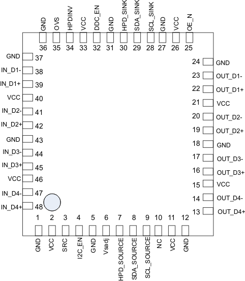
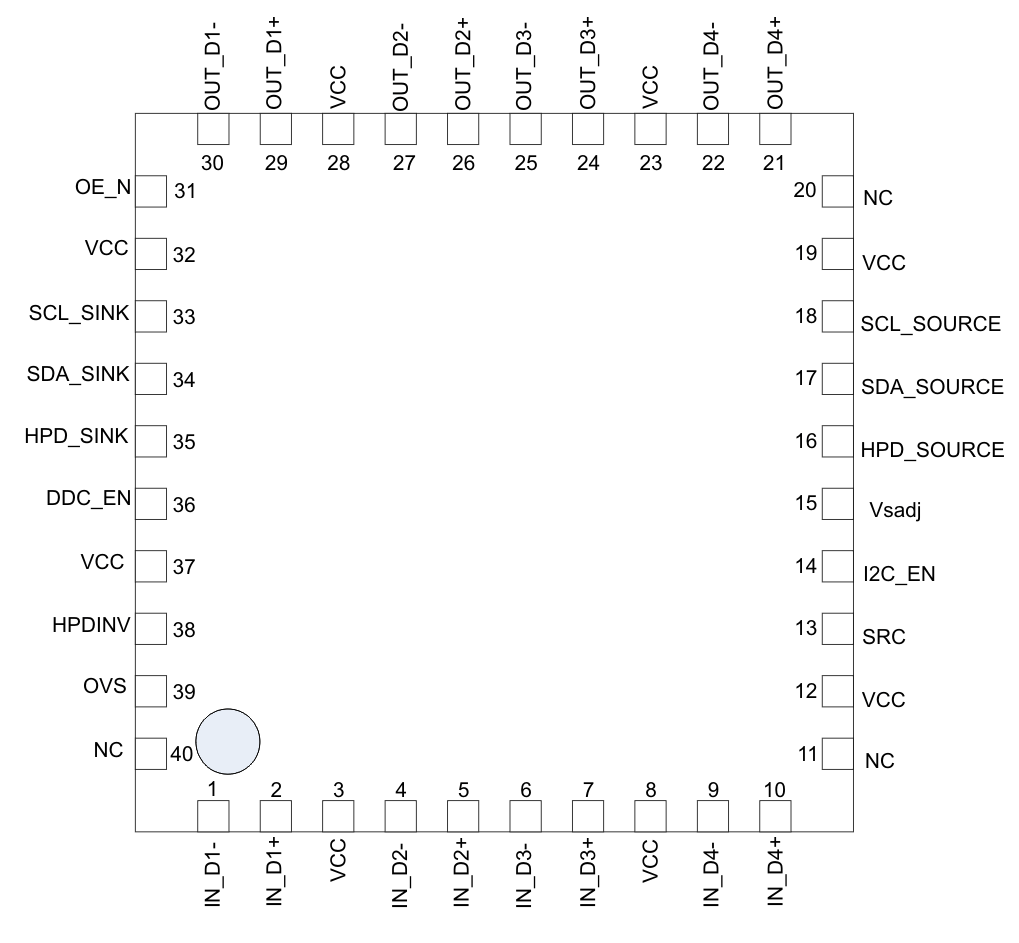
5 Pin Configuration and Functions
48-Pin VQFN
RGZ Package
(Top View)

Pin Functions
| PIN | I/O | DESCRIPTION | ||
|---|---|---|---|---|
| SIGNAL | NO. | |||
| RGZ | RSB | |||
| MAIN LINK INPUT PINS | ||||
| IN_D1 | 38, 39 | 1, 2 | I | DisplayPort Main Link Channel 0 Differential Input |
| IN_D2 | 41, 42 | 4, 5 | I | DisplayPort Main Link Channel 1 Differential Input |
| IN_D3 | 44, 45 | 6, 7 | I | DisplayPort Main Link Channel 2 Differential Input |
| IN_D4 | 47, 48 | 9, 10 | I | DisplayPort Main Link Channel 3 Differential Input |
| MAIN LINK PORT B OUTPUT PINS | ||||
| OUT_D1 | 23, 22 | 30, 29 | O | TMDS Data 2 Differential Output |
| OUT_D2 | 20, 19 | 27, 26 | O | TMDS Data 1 Differential Output |
| OUT_D3 | 17, 16 | 25, 24 | O | TMDS Data 0 Differential Output |
| OUT_D4 | 14, 13 | 22, 21 | O | TMDS Data Clock Differential Output |
| HOT PLUG DETECT PINS | ||||
| HPD_SOURCE | 7 | 16 | O | Hot Plug Detect Output |
| HPD_SINK | 30 | 35 | I | Hot Plug Detect Input |
| AUXILIARY DATA PINS | ||||
| SDA_SOURCE, SCL_SOURCE | 8, 9 | 17, 18 | I/O | Source Side Bidirectional DisplayPort Auxiliary Data Line |
| SDA_SINK, SCL_SINK | 29, 28 | 34, 33 | I/O | TMDS Port Bidirectional DDC Data Lines |
| CONTROL PINS | ||||
| OE_N | 25 | 31 | I | Output Enable and power saving function for High Speed Differential level shifter path. |
| NC | 10 | 11, 20, 40 | No Connect | |
| OVS | 35 | 39 | I | DDC I2C buffer offset select |
| DDC_EN | 32 | 36 | I | Enables or Disables the DDC I2C buffer |
| HPDINV | 34 | 38 | I | HPD_SOURCE Logic and Level Select |
| VSadj | 6 | 15 | I | TMDS Compliant Voltage Swing Control |
| SRC | 3 | 13 | I | TMDS outputs rise and fall time select |
| I2C_EN | 4 | 14 | I | Internal I2C register enable, used for HDMI / DVI connector differentiation |
| SUPPLY AND GROUND PINS | ||||
| VCC | 2, 11, 15, 21, 26, 33, 40, 46 |
3, 8, 12, 19, 23 28, 32, 37 |
3.3 V Supply | |
| GND | 1, 5, 12, 18, 24, 27, 31, 36, 37, 43(1) |
Thermal Pad | Ground | |
(1) Connect the Thermal Pad to GND
Table 1. Control Pin Lookup Table
| SIGNAL | LEVEL(1) | STATE | DESCRIPTION |
|---|---|---|---|
| OE_N | H | Power Saving Mode | Main Link is disabled. IN_Dx termination = 50 Ω with common mode voltage set to 0V. OUT_Dx outputs = high impedance |
| L | Normal Mode | IN_Dx termination = 50 Ω OUT_Dx outputs = active |
|
| I2C_EN | H | HDMI | The Internal I2C register is active and readable when the TMDS port is selected indicating that the connector being used is HDMI. This mode selects the fastest rise and fall time for the TMDS differential output signals |
| L | DVI | The Internal I2C register is disabled and not readable when the TMDS port is selected indicating that the connector being used is DVI. This mode selects a slower rise and fall time for the TMDS differential output signals See Application Information. |
|
| VSadj | 4.02 kΩ ±5% | Output Voltage Swing Contol | Driver output voltage swing precision control to aid with system compliance |
| HPDINV | H | HPD Inversion | HPD_SOURCE VOH =0.9V (typical) and HPD logic is inverted |
| L | HPD non-inversion | HPD_SOURCE VOH =3.2V (typical) and HPD logic is non-inverted | |
| SRC | H | Edge Rate: Slowest | SRC helps to slow down the rise and fall time. SRC =High adds ~60ps to the rise and fall time of the TMDS differential output signals in addition to the I2C_EN pin selection (recommended setting) |
| L | Edge Rate: Slow | SRC helps to slow down the rise and fall time. SRC =Low adds ~30ps to the rise and fall time of the TMDS differential output signals in addition to the I2C_EN pin selection | |
| Hi-Z | Edge Rate | Leaving the SRC pin High Z, will keep the default rise and fall time of the TMDS differential output signals as selected by the I2C_EN pin. It is recommended that an external resistor-divider (less than 100 kΩ) is used so that voltage on this pin = VCC/2, if Hi-Z logic level is intended on this pin. |
|
| OVS | H | Offset 1 | DDC source side VOL and VIL offset range 1 |
| L | Offset 2 | DDC source side VOL and VIL offset range 2 | |
| Hi-Z | Offset 3 | DDC source side VOL and VIL offset range 3 It is recommended that an external resistor-divider (less than 100 kΩ) is used so that voltage on this pin = VCC/2, if Hi-Z logic level is intended on this pin. |
|
| DDC_EN | H | DDC Buffer enabled | DDC Buffer is enabled |
| L | DDC buffer disabled | DDC Buffer is disabled |
