SLLSE12A November 2009 – July 2014 SN75DP119
PRODUCTION DATA.
- 1 Features
- 2 Applications
- 3 Description
- 4 Revision History
- 5 Description (continued)
- 6 Pin Configuration and Functions
- 7 Specifications
- 8 Parameter Measurement Information
- 9 Detailed Description
- 10Application and Implementation
- 11Power Supply Recommendations
- 12Layout
- 13Device and Documentation Support
- 14Mechanical, Packaging, and Orderable Information
封装选项
机械数据 (封装 | 引脚)
散热焊盘机械数据 (封装 | 引脚)
订购信息
7 Specifications
7.1 Absolute Maximum Ratings
over operating free-air temperature range (unless otherwise noted)(1)| MIN | MAX | UNIT | |||
|---|---|---|---|---|---|
| Supply Voltage Range(2) | VCC | –0.3 | 4 | V | |
| Voltage Range | Main Link I/O (OUTx, INx) Differential Voltage | –0.3 | VCC + 0.3 | V | |
| Control Inputs | –0.3 | 5.5 | V | ||
| Continuous power dissipation | See the Thermal Information Table | ||||
(1) Stresses beyond those listed under absolute maximum ratings may cause permanent damage to the device. These are stress ratings only and functional operation of the device at these or any conditions beyond those indicated under recommended operating conditions is not implied. Exposure to absolute-maximum-rated conditions for extended periods may affect device reliability.
(2) All voltage values, except differential voltages, are with respect to network ground terminal.
7.2 Handling Ratings
| MIN | MAX | UNIT | |||
|---|---|---|---|---|---|
| Tstg | Storage temperature range | –65 | 150 | °C | |
| V(ESD) | Electrostatic discharge | Human body model (HBM), per ANSI/ESDA/JEDEC JS-001, all pins(1) | –12 | 12 | kV |
| Charged device model (CDM), per JEDEC specification JESD22-C101, all pins(2) | –1000 | 1000 | V | ||
(1) JEDEC document JEP155 states that 500-V HBM allows safe manufacturing with a standard ESD control process.
(2) JEDEC document JEP157 states that 250-V CDM allows safe manufacturing with a standard ESD control process.
7.3 Recommended Operating Conditions
over operating free-air temperature range (unless otherwise noted)7.4 Thermal Information
| THERMAL METRIC(1) | RGY | RHH | UNIT | |
|---|---|---|---|---|
| 14 PINS | 36 PINS | |||
| RθJA | Junction-to-ambient thermal resistance | 45 | 34 | °C/W |
| RθJC(top) | Junction-to-case (top) thermal resistance | 20 | 20 | |
| RθJB | Junction-to-board thermal resistance | 16 | 17 | |
| ψJT | Junction-to-top characterization parameter | n/a | n/a | |
| ψJB | Junction-to-board characterization parameter | n/a | n/a | |
| RθJC(bot) | Junction-to-case (bottom) thermal resistance | 12 | 12 | |
(1) For more information about traditional and new thermal metrics, see the IC Package Thermal Metrics application report, SPRA953.
7.5 Electrical Characteristics
over recommended operating conditions (unless otherwise noted)| PARAMETER | TEST CONDITIONS | MIN | TYP | MAX | UNIT | |
|---|---|---|---|---|---|---|
| ICCDP1max | Supply current 1 DP lane selected | WorstCase: EN = VCC/2 (1-lane) or VCC (2-lane selected); 2.7Gbps PRBS; VID = 400 mVPP; VOD = 300 mVpp, 8.5 dB pre-emp (PRE_CTL=VCC; VOD_CTL=GND); EQ_CTL = VCC (6 dB); VCC = 3.3 V (for typ) and VCC = 3.6 V (for max), (1) |
16.2 | 21.3 | mA | |
| ICCDP2max | Supply current 2 DP lanes selected | 31.7 | 41.4 | mA | ||
| ICCDP3max | Supply current 1 DP lane selected | EN = VCC/2 (1-lane) or VCC (2-lane selected); 2.7Gbps PRBS; VID = 400 mVPP; VOD = 300 mVPP, 0 dB pre-emp (PRE_CTL = GND); VOD_CTL = VCC/2); EQ_CTL=GND (0 dB); VCC = 3.3 V (for typ) and VCC = 3.6 V (for max), |
12.9 | 17.6 | mA | |
| ICCDP4max | Supply current 2 DP lanes selected | 24.9 | 34.1 | mA | ||
| ICCDP1typ | Supply current 1 DP lane selected | EN = VCC/2 (1-lane) or VCC (2-lane selected); 2.7Gbps PRBS; IN/OUT; VID = 600 mVPP; (PRE_CTL=GND); VOD_CTL = VCC); VCC = 3.3 V, EQ_CTL = GND (no EQ) (2) |
14.5 | mA | ||
| ICCDP2typ | Supply current 2 DP lanes selected | 28.2 | mA | |||
| ICCDP3typ | Supply current 1 DP lane selected | EN = VCC/2 (1-lane) or VCC (2-lane selected); 2.7Gbps PRBS; no pre-emp; IN/OUT; VID = 800 mVPP; (PRE_CTL= VOD_CTL = VCC); VCC = 3.3 V, EQ_CT L = GND (no EQ) (3) |
14.5 | mA | ||
| ICCDP4typ | Supply current 2 DP lanes selected | 28.2 | mA | |||
| IPWRDN | Shutdown current (PWRDN mode) | EN = GND; | 25 | 100 | µA | |
| 3-LEVEL CONTROL PINS (EN, VOD_CTL, PRE_CTL, EQ_CTL) | ||||||
| IL | Low-level input current | VI = 0.5 V; VCC = 3.6 V | –30 | 30 | µA | |
| IH | High-level input current | VI = VCC – 0.5 V; Vcc = 3.6V | –30 | 30 | µA | |
| IM | Mid-level input current | VI = VCC /2 – 0.3V and VI = VCC /2 + 0.3 V; VCC = 3.6 V | –30 | 30 | µA | |
| Rbias | Input bias resistance | See Figure 6 | 105 | 125 | 145 | kΩ |
| RESD | input series resistance to biasing network | See Figure 6 | 2 | 2.4 | kΩ | |
| IN[1:0], OUT[1:0] (4) | ||||||
| [VOD(0.3)] | Output differential voltage swing | VPRE = VPRE(0.0); 675 Mbps D10.2 test pattern; VID = 300 mVpp; EQ = 3 dB |
300mV setting only used with pre-emphasis | |||
| [300] | mVpp | |||||
| VOD(0.4) | 400 | mVpp | ||||
| VOD(0.6) | 600 | mVpp | ||||
| VOD(0.75) | 800 | mVpp | ||||
| VEyemask | Eyemask compliance | VOD = 800 mVpp test pattern measured in compliance with PHY CTS1.1 section 3.1 at test point TP2; VID= 300mVPP ; EQ=3dB | pass | |||
| VPRE(0.0) | Driver output pre-emphasis | VOD = VOD(0.4), VOD(0.6), or VOD(0.8) at 2.7Gbps only | 0 | dB | ||
| VPRE(2.5) | VOD = VOD(0.3) or VOD(0.6) at 2.7Gbps only | 2.7 | dB | |||
| VPRE(3.5) | VOD = VOD(0.4) at 2.7Gbps only; EQ=3dB | 0.9 | 3.5 | dB | ||
| VPRE(6.0) | VOD = VOD(0.3) or VOD(0.4) at 2.7Gbps only; EQ=3dB | 3.3 | 6.0 | dB | ||
| VPRE(8.5) | VOD = VOD(0.3) at 2.7Gbps only; EQ=3dB | 7 | 8.5 | dB | ||
| ROUT | Driver output impedance (single ended) | 100 | Ω | |||
| RIN | Differential input termination impedance | 80 | 100 | 120 | Ω | |
| VItem | Input termination voltage (AC coupled) | Self-biased | 0 | 1.7 | 2 | V |
| VOCM | Output common mode voltage | 0 | 1.55 | 2 | V | |
| VTXACCM | Output AC common mode voltage | Verified through statistical measurements only using 1.62Gbps and 2.7Gbps PRBS7 data pattern measured at TP2; EQ = 3dB | 20 | mVrms | ||
| ITXSHORT | Output short circuit current limit | OUT[1:0] shorted to GND; single-ended current | 50 | mA | ||
| IRXSHORT | Input short circuit current limit | IN[1:0] shorted to GND (single ended) | 50 | mA | ||
(1) This current consumption also applies to VOD = 400mV with 5.5 dB pre-emphasis or VOD = 600mV output swing and 2dB pre-emphasis
(2) This current consumption also applies to VOD = 300mV with 2 dB pre-emphasis
(3) This current consumption also applies to VOD = 300mV with 6dB pre-emphasis or VOD = 400mV output swing and 3.5dB pre-emphasis
(4) The SN75DP119 is designed to support the DisplayPort high speed differential main link with three levels of output voltage swing and three levels of pre-emphasis. The main link I/Os of the SN75DP119 are designed to be compliant with the DisplayPort 1.1a specification
7.6 Switching Characteristics
over recommended operating conditions (unless otherwise noted)| PARAMETER | TEST CONDITIONS | MIN | TYP | MAX | UNIT | |
|---|---|---|---|---|---|---|
| tR/F(DP) | Differential output edge rate (20%–80%) | All VOD options, Measured at TP1, PRBS7; VID = 300 mVPP; EQ = 3dB; CLOAD = 1 pF |
50 | 155 | ps | |
| tPD | Propagation delay time | 325 | 550 | ps | ||
| tskpp | Part-to-Part skew | With identical voltage and temperature | 0 | 160 | ps | |
| tSK(1) | Intra-pair output skew | Signal input skew = 0ps; dR = 2.7Gbps, No Pre-emphasis, 800 mVp-p , D10.2 pattern | 20 | ps | ||
| tSK(2) | Inter-pair output skew | 100 | ps | |||
| ΔtDPJIT(PP) | Peak-to-peak output residual jitter at package pins | VOD(0.4); VPRE(0.0); Δtjit = tjit(output) – tjit(input); verified through design simulation and statistical measurements only using 1.62Gbps and 2.7Gbps PRBS7 data pattern. | 15 | ps | ||
7.7 Typical Characteristics
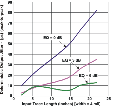 Figure 1. Deterministic Output Jitter vs Input Trace Length