SCES224R April 1999 – January 2015 SN74LVC1G126
PRODUCTION DATA.
- 1 Applications
- 2 Simplified Schematic
- 3 Revision History
- 4 Pin Configuration and Functions
- 5 Specifications
- 6 Parameter Measurement Information
- 7 Detailed Description
- 8 Application and Implementation
- 9 Power Supply Recommendations
- 10Layout
- 11Device and Documentation Support
- 12Mechanical, Packaging, and Orderable Information
封装选项
请参考 PDF 数据表获取器件具体的封装图。
机械数据 (封装 | 引脚)
- DBV|5
- DSF|6
- DCK|5
- DRL|5
- DRY|6
- YZP|5
散热焊盘机械数据 (封装 | 引脚)
- DRY|6
订购信息
8 Application and Implementation
NOTE
Information in the following applications sections is not part of the TI component specification, and TI does not warrant its accuracy or completeness. TI’s customers are responsible for determining suitability of components for their purposes. Customers should validate and test their design implementation to confirm system functionality.
8.1 Application Information
The SN74LVC1G126 device is a high-drive CMOS device that can be used as an output enabled buffer with a high output drive, such as an LED application. It can produce 24 mA of drive current at 3.3 V, making it ideal for driving multiple outputs and good for high speed applications up to 100 MHz. The inputs are 5.5-V tolerant allowing it to translate down to VCC.
8.2 Typical Application
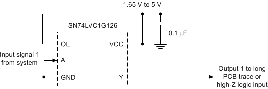 Figure 5. Application Schematic
8.2.1 Design Requirements
This device uses CMOS technology and has balanced output drive. Care should be taken to avoid bus contention because it can drive currents that would exceed maximum limits. Outputs can be combined to produce higher drive but the high drive will also create faster edges into light loads, so routing and load conditions should be considered to prevent ringing.
8.2.2 Detailed Design Procedure
- Recommended Input Conditions:
- For rise time and fall time specifications, see Δt/ΔV in the Recommended Operating Conditions table.
- For specified high and low levels, see VIH and VIL in the Recommended Operating Conditions table.
- Inputs are overvoltage tolerant allowing them to go as high as 5.5 V at any valid VCC.
- Recommend Output Conditions:
- Load currents should not exceed 50 mA per output and 100 mA total for the part.
8.2.3 Application Curves
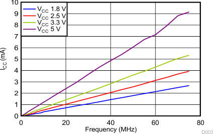 Figure 6. ICC vs Frequency