SCAS289M January 1993 – December 2014 SN74LVC112A
PRODUCTION DATA.
- 1 Features
- 2 Applications
- 3 Description
- 4 Simplified Schematic
- 5 Revision History
- 6 Pin Configuration and Functions
-
7 Specifications
- 7.1 Absolute Maximum Ratings
- 7.2 ESD Ratings
- 7.3 Recommended Operating Conditions
- 7.4 Thermal Information
- 7.5 Electrical Characteristics
- 7.6 Timing Requirements, -40°C to 85°C
- 7.7 Timing Requirements, -40°C to 125°C
- 7.8 Switching Characteristics, -40°C to 85°C
- 7.9 Switching Characteristics, -40°C to 125°C
- 7.10 Operating Characteristics
- 7.11 Typical Characteristics
- 8 Parameter Measurement Information
- 9 Detailed Description
- 10Application and Implementation
- 11Power Supply Recommendations
- 12Layout
- 13Device and Documentation Support
- 14Mechanical, Packaging, and Orderable Information
封装选项
请参考 PDF 数据表获取器件具体的封装图。
机械数据 (封装 | 引脚)
- PW|16
- DB|16
- NS|16
- D|16
- DGV|16
散热焊盘机械数据 (封装 | 引脚)
订购信息
9 Detailed Description
9.1 Overview
This dual negative-edge-triggered J-K flip-flop is designed for 1.65-V to 3.6-V VCC operation.
A low level at the preset (PRE) or clear (CLR) inputs sets or resets the outputs, regardless of the levels of the other inputs. When PRE and CLR are inactive (high), data at the J and K inputs meeting the setup-time requirements is transferred to the outputs on the negative-going edge of the clock pulse. Clock triggering occurs at a voltage level and is not directly related to the rise time of the clock pulse. Following the hold-time interval, data at the J and K inputs can be changed without affecting the levels at the outputs. The SN74LVC112A can perform as a toggle flip-flop by tying J and K high.
Inputs can be driven from either 3.3-V or 5-V devices. This feature allows the use of these devices as translators in a mixed 3.3-V/5-V system environment.
9.2 Functional Block Diagram
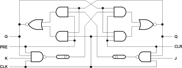 Figure 4. Logic Diagram, Each Flip-Flop (Positive Logic)
9.3 Feature Description
- Wide operating voltage range
- Operates from 1.65 V to 3.6 V
- Allows down voltage translation
- Inputs accept voltages to 5.5 V
- Ioff feature
- Allows voltages on the inputs and outputs when VCC is 0 V
9.4 Device Functional Modes
Table 1. Function Table
| INPUTS | OUTPUTS | |||||
|---|---|---|---|---|---|---|
| PRE | CLR | CLK | J | K | Q | Q |
| L | H | X | X | X | H | L |
| H | L | X | X | X | L | H |
| L | L | X | X | X | H(1) | H(1) |
| H | H | ↓ | L | L | Q0 | Q0 |
| H | H | ↓ | H | L | H | L |
| H | H | ↓ | L | H | L | H |
| H | H | ↓ | H | H | Toggle | |
| H | H | H | X | X | Q0 | Q0 |