SCLS381M August 1997 – March 2015 SN74LV74A
UNLESS OTHERWISE NOTED, this document contains PRODUCTION DATA.
- 1 Features
- 2 Applications
- 3 Description
- 4 Revision History
- 5 Pin Configuration and Functions
-
6 Specifications
- 6.1 Absolute Maximum Ratings
- 6.2 ESD Ratings
- 6.3 Recommended Operating Conditions
- 6.4 Electrical Characteristics
- 6.5 Switching Characteristics: VCC = 2.5 V ± 0.2 V
- 6.6 Switching Characteristics: VCC = 3.3 V ± 0.3 V
- 6.7 Switching Characteristics: VCC = 5 V ± 0.5 V
- 6.8 Timing Requirements: VCC = 2.5 V ± 0.2 V
- 6.9 Timing Requirements: VCC = 3.3 V ± 0.3 V
- 6.10 Timing Requirements: VCC = 5 V ± 0.5 V
- 6.11 Noise Characteristics
- 6.12 Operating Characteristics
- 6.13 Typical Characteristics
- 7 Parameter Measurement Information
- 8 Detailed Description
- 9 Application and Implementation
- 10Power Supply Recommendations
- 11Layout
- 12Device and Documentation Support
- 13Mechanical, Packaging, and Orderable Information
封装选项
请参考 PDF 数据表获取器件具体的封装图。
机械数据 (封装 | 引脚)
- D|14
- RGY|14
- DGV|14
- PW|14
- DB|14
- NS|14
散热焊盘机械数据 (封装 | 引脚)
- RGY|14
订购信息
8 Detailed Description
8.1 Overview
These dual positive-edge-triggered D-type flip-flops are designed for 2-V to 5.5-V VCC operation.
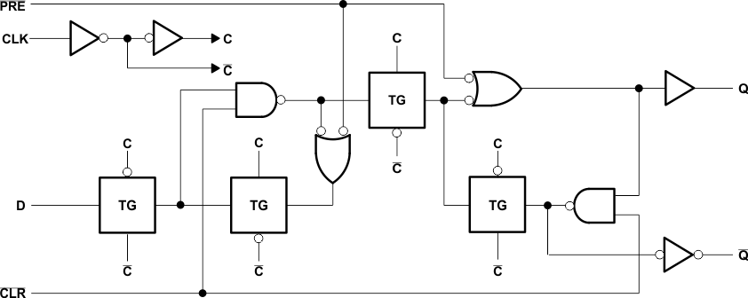
A low level at the preset (PRE) or clear (CLR) inputs sets or resets the outputs, regardless of the levels of the other inputs. When PRE and CLR are inactive (high), data at the data (D) inputs meeting the setup-time requirements is transferred to the outputs on the positive-going edge of the clock pulse. Clock triggering occurs at a voltage level and is not directly related to the rise time of the clock pulse. Following the hold-time interval, data at the D input can be changed without affecting the levels at the outputs. The state of the output upon power-up is not known until the first valid clock edge has occurred while VCC is within Recommended Operating Conditions.
These devices are fully specified for partial-power-down applications using Ioff. The Ioff circuitry disables the outputs, preventing damaging current backflow through the devices when they are powered down.
8.2 Functional Block Diagram
 Figure 4. Logic Diagram, Each Flip-Flop (Positive Logic)
8.3 Feature Description
The device’s wide operating range allows it to be used in a variety of systems that use different logic levels. The low propagation delay allows fast switching and higher speeds of operation. In addition, the low ground bounce stabilizes the performance of non-switching outputs while another output is switching.