ZHCSQR2G August 2003 – March 2023 SN74LV595A-Q1
PRODMIX
- 1 特性
- 2 应用
- 3 说明
- 4 Revision History
- 5 Pin Configuration and Functions
-
6 Specifications
- 6.1 Absolute Maximum Ratings
- 6.2 ESD Ratings
- 6.3 Recommended Operating Conditions
- 6.4 Thermal Information
- 6.5 Electrical Characteristics
- 6.6 Timing Requirements, VCC = 2.5 V ± 0.2 V
- 6.7 Timing Requirements, VCC = 3.3 V ± 0.3 V
- 6.8 Timing Requirements, VCC = 5 V ± 0.5 V
- 6.9 Switching Characteristics, VCC = 2.5 V ± 0.2 V
- 6.10 Switching Characteristics, VCC = 3.3 V ± 0.3 V
- 6.11 Switching Characteristics, VCC = 5 V ± 0.5 V
- 6.12 Timing Diagrams
- 6.13 Noise Characteristics
- 6.14 Operating Characteristics
- 6.15 Typical Characteristics
- 7 Parameter Measurement Information
- 8 Detailed Description
- 9 Application and Implementation
- 10Device and Documentation Support
- 11Mechanical, Packaging, and Orderable Information
封装选项
机械数据 (封装 | 引脚)
散热焊盘机械数据 (封装 | 引脚)
- BQB|16
订购信息
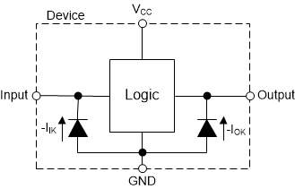
8.3.5 Clamp Diode Structure
Figure 8-3 shows the inputs and outputs to this device have negative clamping diodes only.
CAUTION: Voltages beyond the values
specified in the Absolute Maximum Ratings table can cause damage to the device. The
input and output voltage ratings may be exceeded if the input and output clamp-current
ratings are observed.
 Figure 8-3 Electrical Placement of Clamping
Diodes for Each Input and Output