SCLS388K September 1997 – December 2014 SN74LV04A
PRODUCTION DATA.
- 1 Features
- 2 Applications
- 3 Description
- 4 Simplified Schematic
- 5 Revision History
- 6 Pin Configuration and Functions
-
7 Specifications
- 7.1 Absolute Maximum Ratings
- 7.2 ESD Ratings
- 7.3 Recommended Operating Conditions
- 7.4 Thermal Information
- 7.5 Electrical Characteristics
- 7.6 Switching Characteristics, VCC = 2.5 V ± 0.2 V
- 7.7 Switching Characteristics, VCC = 3.3 V ± 0.3 V
- 7.8 Switching Characteristics, VCC = 5 V ± 0.5 V
- 7.9 Noise Characteristics
- 7.10 Operating Characteristics
- 7.11 Typical Characteristics
- 8 Parameter Measurement Information
- 9 Detailed Description
- 10Application and Implementation
- 11Power Supply Recommendations
- 12Layout
- 13Device and Documentation Support
- 14Mechanical, Packaging, and Orderable Information
封装选项
请参考 PDF 数据表获取器件具体的封装图。
机械数据 (封装 | 引脚)
- D|14
- RGY|14
- DGV|14
- DB|14
- PW|14
- NS|14
散热焊盘机械数据 (封装 | 引脚)
- RGY|14
订购信息
9 Detailed Description
9.1 Overview
These hex inverters are designed for 2-V to 5.5-V VCC operation. The SN74LV04A devices contain six independent inverters. These devices perform the Boolean function Y = A.
These devices are fully specified for partial-power-down applications using Ioff. The Ioff circuitry disables the outputs, preventing damaging current backflow through the devices when they are powered down.
The inputs are high impedance when VCC = 0V.
9.2 Functional Block Diagram
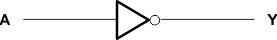 Figure 4. Logic Diagram Each Inverter (Positive Logic)
9.3 Feature Description
- Wide operating voltage range
- Operates from 2 V to 5.5 V
- Allows down-voltage translation
- Inputs accept voltages to 5.5 V
- Ioff feature
- Supports Live Insertion, Partial Power DownMode, and Back Drive Protection
9.4 Device Functional Modes
Table 1. Function Table
(Each Inverter)
| INPUT A |
OUTPUT Y |
|---|---|
| H | L |
| L | H |