ZHCSKE5 October   2019 SN74HCS72-Q1

PRODUCTION DATA.  

  1. 特性
  2. 应用
  3. 说明
    1.     Device Images
      1.      施密特触发输入的优势
  4. 修订历史记录
  5. Pin Configuration and Functions
    1.     Pin Functions
  6. Specifications
    1. 6.1 Absolute Maximum Ratings
    2. 6.2 ESD Ratings
    3. 6.3 Recommended Operating Conditions
    4. 6.4 Thermal Information
    5. 6.5 Electrical Characteristics
    6. 6.6 Switching Characteristics
    7. 6.7 Timing Characteristics
    8. 6.8 Typical Characteristics
  7. Parameter Measurement Information
  8. Detailed Description
    1. 8.1 Overview
    2. 8.2 Functional Block Diagram
    3. 8.3 Feature Description
      1. 8.3.1 Balanced CMOS Push-Pull Outputs
      2. 8.3.2 CMOS Schmitt-Trigger Inputs
      3. 8.3.3 Positive and Negative Clamping Diodes
    4. 8.4 Device Functional Modes
  9. Application and Implementation
    1. 9.1 Application Information
    2. 9.2 Typical Application
      1. 9.2.1 Design Requirements
        1. 9.2.1.1 Output Considerations
        2. 9.2.1.2 Input Considerations
        3. 9.2.1.3 Timing Considerations
      2. 9.2.2 Detailed Design Procedure
      3. 9.2.3 Application Curve
  10. 10Power Supply Recommendations
  11. 11Layout
    1. 11.1 Layout Guidelines
    2. 11.2 Layout Example
  12. 12器件和文档支持
    1. 12.1 文档支持
      1. 12.1.1 相关文档
    2. 12.2 接收文档更新通知
    3. 12.3 社区资源
    4. 12.4 商标
    5. 12.5 静电放电警告
    6. 12.6 Glossary
  13. 13机械、封装和可订购信息

封装选项

机械数据 (封装 | 引脚)
散热焊盘机械数据 (封装 | 引脚)
订购信息

Pin Configuration and Functions

D and PW Package
14-Pin SOIC and TSSOP
Top View
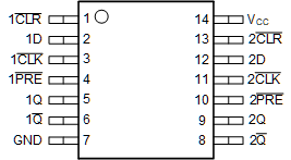
SN74HCS72-Q1 package-pinout-diagram.gif

Pin Functions

PIN TYPE DESCRIPTION
NAME NO.
1CLR 1 Input Clear for channel 1, active low
1D 2 Input Data for channel 1
1CLK 3 Input Clock for channel 1, falling edge triggered
1PRE 4 Input Preset for channel 1, active low
1Q 5 Output Output for channel 1
1Q 6 Output Inverted output for channel 1
GND 7 Ground
2Q 8 Output Inverted output for channel 2
2Q 9 Output Output for channel 2
2PRE 10 Input Preset for channel 2, active low
2CLK 11 Input Clock for channel 2, falling edge triggered
2D 12 Input Data for channel 2
2CLR 13 Input Clear for channel 2, active low
VCC 14 Positive supply