ZHCSR32A September 2004 – December 2022 SN74CBT3383C
PRODUCTION DATA
- 1 特性
- 2 应用
- 3 说明
- 4 Revision History
- 5 说明(续)
- 6 Pin Configuration and Functions
- 7 Specifications
- 8 Parameter Measurement Information
- 9 Detailed Description
- 10Application and Implementation
- 11Power Supply Recommendations
- 12Layout
- 13Device and Documentation Support
- 14Mechanical, Packaging, and Orderable Information
封装选项
请参考 PDF 数据表获取器件具体的封装图。
机械数据 (封装 | 引脚)
- DBQ|24
- DW|24
- PW|24
散热焊盘机械数据 (封装 | 引脚)
订购信息
8 Parameter Measurement Information
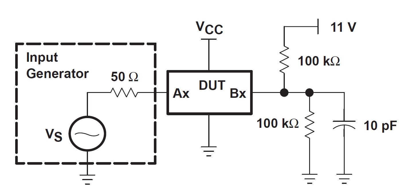
 Figure 8-1 Device Test Setup
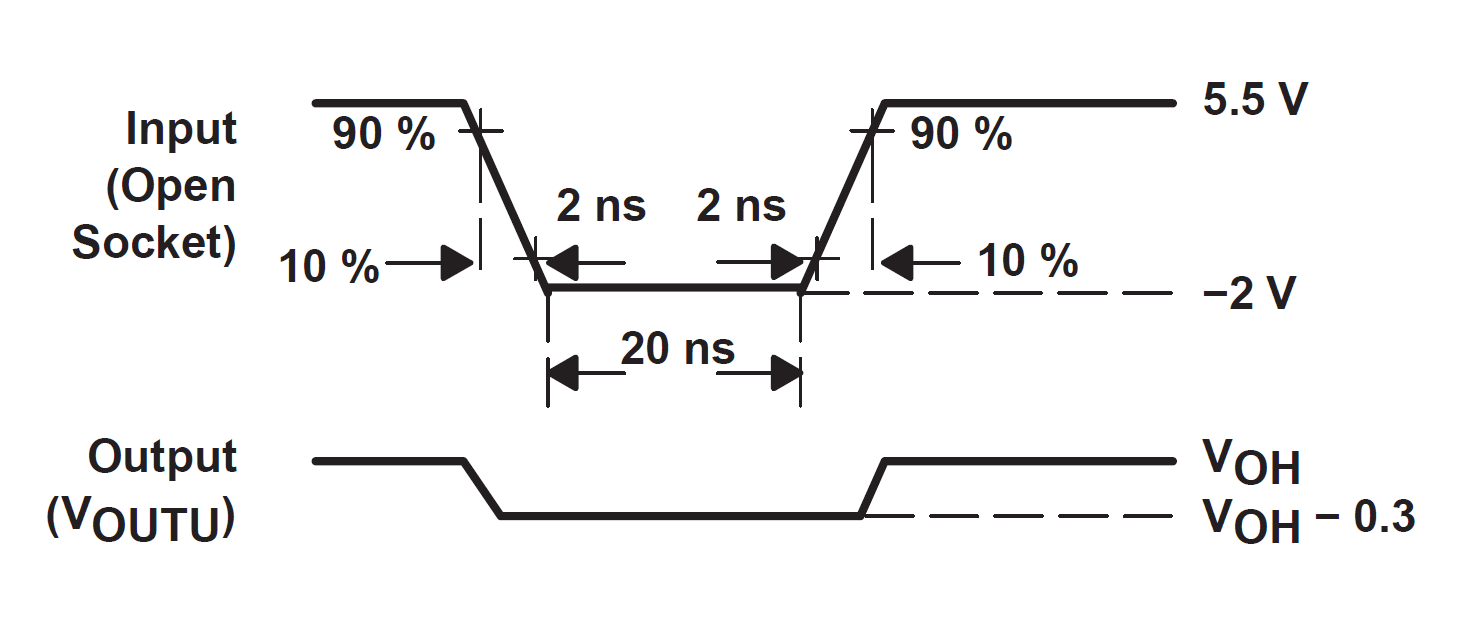
 Figure 8-2 Transient Input Voltage
(VI) and Output Voltage (VOUTU) Waveforms (Switch
OFF)
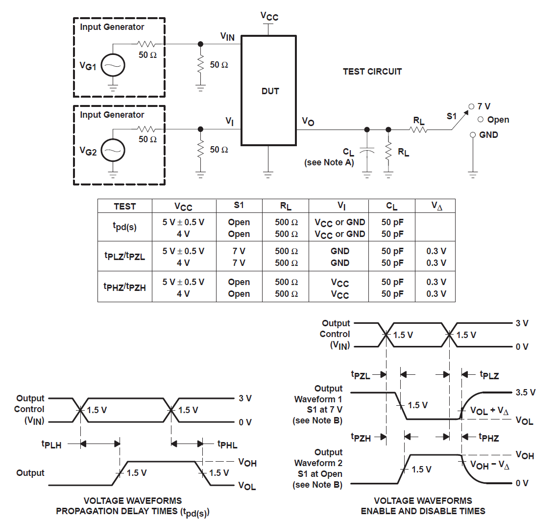
A. CL includes probe and jig capacitance.
B. Waveform 1 is for an output with internal conditions such that the output is
low, except when disabled by the output control. Waveform 2 is for an output
with internal conditions such that the output is high, except when disabled by
the output control.
C. All
input pulses are supplied by generators having the following characteristics:
PRR ≤ 10 MHz, ZO = 50 Ω, tr ≤ 2.5 ns, tf ≤ 2.5
ns.
D. The
outputs are measured one at a time, with one transition per measurement.
E. tPLZ and tPHZ are the same as tdis.
F. tPZL and tPZH are the same as ten.
G. tPLH and tPHL are the same as one or more
tpds. The tpd propagation delay is the calculated RC time
constant of the typical ON-state resistance of the switch and the specified load
capacitance, when driven by an ideal voltage source (zero output impedance).
H. All
parameters and waveforms are not applicable to all devices.
Figure 8-3 Test Circuit and Voltage
Waveforms