SCDS119C january 2003 – December 2015 SN74CB3T3306
PRODUCTION DATA.
- 1 Features
- 2 Applications
- 3 Description
- 4 Revision History
- 5 Pin Configuration and Functions
- 6 Specifications
- 7 Parameter Measurement Information
- 8 Detailed Description
- 9 Application and Implementation
- 10Power Supply Recommendations
- 11Layout
- 12Device and Documentation Support
- 13Mechanical, Packaging, and Orderable Information
8 Detailed Description
8.1 Overview
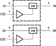
The SN74CB3T3306 device is organized as two 1-bit bus switches with separate ouput-enable (1OE, 2OE) inputs. It can be used as two 1-bit bus switches or as one 2-bit bus switch. When OE is low, the associated 1-bit bus switch is ON, and the A port is connected to the B port, allowing bidirectional data flow between ports. When OE is high, the associated 1-bit bus switch is OFF, and a high-impedance state exists between the A and B ports.
This device is fully specified for partial-power-down applications using Ioff. The Ioff feature ensures that damaging current will not backflow through the device when it is powered down. The SN74CB3T3306 device has isolation during power off.
To ensure the high-impedance state during power up or power down, OE should be tied to VCC through a pullup resistor; the minimum value of the resistor is determined by the current-sinking capability of the driver.
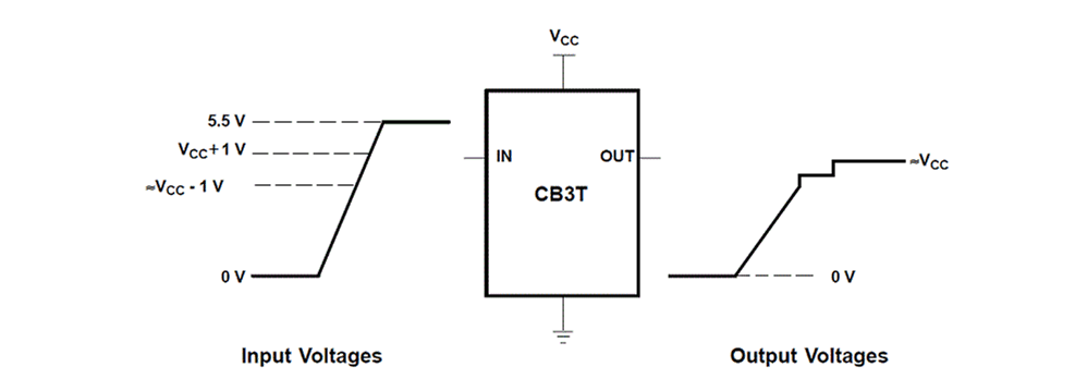
 Figure 5. Typical DC Voltage-Translation Characteristics
8.2 Functional Block Diagrams
 Figure 6. Functional Block Diagram, SN74CB3T3306
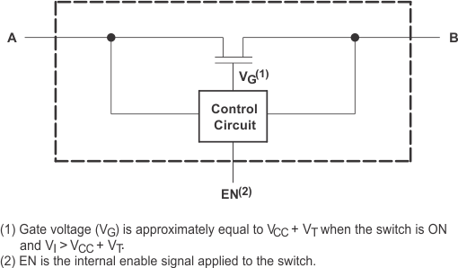
 Figure 7. Simplified Schematic, Each FET Switch (SW)
8.3 Feature Description
The SN74CB3T3306 is ideal for low-power portable equipment. Power consumption is low by design, ICC =
20 μA, On-state resistance is low (ron = 5 Ω) It has bidirectional data flow with near zero propagation delay. The devices minimizes loading due to the low input/output capacitance Cio(OFF) = 4.5 pF Typ. Operating VCC range from 2.3 V to 3.6 V. The output tracks VCC.Data and control inputs provide undershoot clamp diodes. Control inputs can be driven by TTL or 5-V/3.3-V CMOS outputs. It supports mixed-mode signal operation on all data I/O ports. Data I/Os support 0- to 5-V signaling levels (0.8 V, 1.2 V, 1.5 V, 1.8 V, 2.5 V, 3.3 V, 5 V). The device is protected from damaging current, Ioff supports partial shutdown which prevents the current from flowing back through the device when it is powered down. In addition, it has 5-V tolerant I/Os with device powered up or powered down. The device is latch-up resistant with 250 mA exceeding the JESD 17 standard, providing protection from destruction due to latch-up. This device is protected against electrostatic discharge. It is tested per JESD 22 using 2000-V Human-Body Model (A114-B, Class II), and 1000-V Charged-Device Model (C101).
8.4 Device Functional Modes
Table 1 lists the functional modes for the SN74CB3T3306.
Table 1. Function Table
| INPUT OE |
INPUT/OUTPUT A |
FUNCTION |
|---|---|---|
| L | B | A port = B port |
| H | Hi-Z | Disconnect |