SCDS168A May 2004 – September 2015 SN74CB3Q16244
PRODUCTION DATA.
- 1 Features
- 2 Applications
- 3 Description
- 4 Revision History
- 5 Description continued
- 6 Pin Configuration and Functions
- 7 Specifications
- 8 Parameter Measurement Information
- 9 Detailed Description
- 10Application and Implementation
- 11Power Supply Recommendations
- 12Layout
- 13Device and Documentation Support
- 14Mechanical, Packaging, and Orderable Information
封装选项
请参考 PDF 数据表获取器件具体的封装图。
机械数据 (封装 | 引脚)
- DGG|48
- DL|48
- DGV|48
散热焊盘机械数据 (封装 | 引脚)
订购信息
10 Application and Implementation
NOTE
Information in the following applications sections is not part of the TI component specification, and TI does not warrant its accuracy or completeness. TI’s customers are responsible for determining suitability of components for their purposes. Customers should validate and test their design implementation to confirm system functionality.
10.1 Application Information
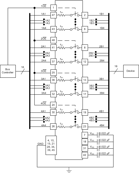
The SN74CB3Q16244 device can be used to control up to 16 bits with 4 channels simultaneously.
10.2 Typical Application
The application shown in Figure 5 is a 16-bit bus being controlled. The OE pins are used to control the chip from the bus controller. This is a generic example and can apply to many situations. If an application requires fewer than 16 bits, ensure that the A side is tied either high or low on unused channels.
 Figure 5. Typical Application of the SN74CB3Q16244
10.2.1 Design Requirements
A 0.022-µF bypass capacitor should be placed between each VCC pin and GND. Each capacitor must be placed as close as possible to the SN74CB3Q16244 device.
10.2.2 Detailed Design Procedure
- Recommended input conditions:
- For specified high and low levels, see VIH and VIL in Recommended Operating Conditions
- Inputs and outputs are overvoltage tolerant, which allows them to go as high as 5.5 V at any valid VCC
- Recommended output conditions:
- Load currents must not exceed ±64 mA per channel
- Frequency selection criterion:
- Added trace resistance or capacitance can reduce maximum frequency capability; use layout practices as directed in Layout
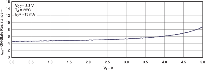
10.2.3 Application Curve
 Figure 6. Typical ron vs VI