ZHCSJI7 March 2019 SN74AXCH4T245
PRODUCTION DATA.
- 1 特性
- 2 应用
- 3 说明
- 4 修订历史记录
- 5 Pin Configuration and Functions
-
6 Specifications
- 6.1 Absolute Maximum Ratings
- 6.2 ESD Ratings
- 6.3 Recommended Operating Conditions
- 6.4 Thermal Information
- 6.5 Electrical Characteristics
- 6.6 Switching Characteristics, VCCA = 0.7 ± 0.05 V
- 6.7 Switching Characteristics, VCCA = 0.8 ± 0.04 V
- 6.8 Switching Characteristics, VCCA = 0.9 ± 0.045 V
- 6.9 Switching Characteristics, VCCA = 1.2 ± 0.1 V
- 6.10 Switching Characteristics, VCCA = 1.5 ± 0.1 V
- 6.11 Switching Characteristics, VCCA = 1.8 ± 0.15 V
- 6.12 Switching Characteristics, VCCA = 2.5 ± 0.2 V
- 6.13 Switching Characteristics, VCCA = 3.3 ± 0.3 V
- 6.14 Operating Characteristics: TA = 25°C
- 6.15 Typical Characteristics
- 7 Parameter Measurement Information
-
8 Detailed Description
- 8.1 Overview
- 8.2 Functional Block Diagram
- 8.3
Feature Description
- 8.3.1 Standard CMOS Inputs
- 8.3.2 Balanced High-Drive CMOS Push-Pull Outputs
- 8.3.3 Partial Power Down (Ioff)
- 8.3.4 VCC Isolation
- 8.3.5 Over-voltage Tolerant Inputs
- 8.3.6 Glitch-free Power Supply Sequencing
- 8.3.7 Negative Clamping Diodes
- 8.3.8 Fully Configurable Dual-Rail Design
- 8.3.9 Supports High-Speed Translation
- 8.3.10 Bus-Hold Data Inputs
- 8.4 Device Functional Modes
- 9 Application and Implementation
- 10Power Supply Recommendations
- 11Layout
- 12器件和文档支持
- 13机械、封装和可订购信息
封装选项
机械数据 (封装 | 引脚)
散热焊盘机械数据 (封装 | 引脚)
- RSV|16
订购信息
7.1 Load Circuit and Voltage Waveforms
Unless otherwise noted, all input pulses are supplied by generators having the following characteristics:
- f = 1 MHz
- ZO = 50 Ω
- dv/dt ≤ 1 ns/V

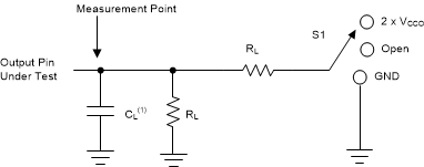
1. CL includes probe and jig capacitance.
Figure 5. Load Circuit Table 1. Load Circuit Conditions
| Parameter | VCCO | RL | CL | S1 | VTP | |
|---|---|---|---|---|---|---|
| Δt/Δv | Input transition rise or fall rate | 0.65 V – 3.6 V | 1 MΩ | 15 pF | Open | N/A |
| tpd | Propagation (delay) time | 1.1 V – 3.6 V | 2 kΩ | 15 pF | Open | N/A |
| 0.65 V – 0.95 V | 20 kΩ | 15 pF | Open | N/A | ||
| ten, tdis | Enable time, disable time | 3 V – 3.6 V | 2 kΩ | 15 pF | 2 × VCCO | 0.3 V |
| 1.65 V – 2.7 V | 2 kΩ | 15 pF | 2 × VCCO | 0.15 V | ||
| 1.1 V – 1.6 V | 2 kΩ | 15 pF | 2 × VCCO | 0.1 V | ||
| 0.65 V – 0.95 V | 20 kΩ | 15 pF | 2 × VCCO | 0.1 V | ||
| ten, tdis | Enable time, disable time | 3 V – 3.6 V | 2 kΩ | 15 pF | GND | 0.3 V |
| 1.65 V – 2.7 V | 2 kΩ | 15 pF | GND | 0.15 V | ||
| 1.1 V – 1.6 V | 2 kΩ | 15 pF | GND | 0.1 V | ||
| 0.65 V – 0.95 V | 20 kΩ | 15 pF | GND | 0.1 V | ||

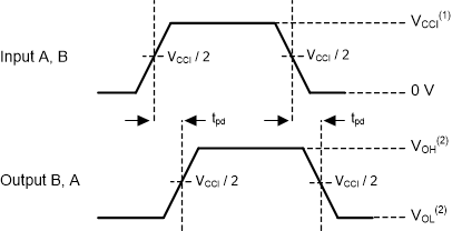
- VCCI is the supply pin associated with the input port.
- VOH and VOL are typical output voltage levels that occur with specified RL, CL, and S1

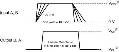
- VCCI is the supply pin associated with the input port.
- VOH and VOL are typical output voltage levels that occur with specified RL, CL, and S1

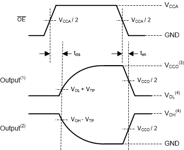
1. Output waveform on the condition that input is driven to a valid Logic Low.
2. Output waveform on the condition that input is driven to a valid Logic High.
3. VCCO is the supply pin associated with the output port.
4. VOH and VOL are typical output voltage levels with specified RL, CL, and S1.
Figure 8. Enable Time and Disable Time