SCAS416Q March 1994 – September 2016 SN74ALVC164245
PRODUCTION DATA.
- 1 Features
- 2 Applications
- 3 Description
- 4 Revision History
- 5 Pin Configuration and Functions
-
6 Specifications
- 6.1 Absolute Maximum Ratings
- 6.2 ESD Ratings
- 6.3 Recommended Operating Conditions: VCCB at 3.3 V
- 6.4 Recommended Operating Conditions: VCCA at 2.5 V
- 6.5 Thermal Information
- 6.6 Electrical Characteristics: VCCA = 2.7 V to 3.6 V
- 6.7 Electrical Characteristics: VCCA = 2.3 V to 2.7 V
- 6.8 Switching Characteristics
- 6.9 Operating Characteristics
- 6.10 Typical Characteristics
- 7 Parameter Measurement Information
- 8 Detailed Description
- 9 Application and Implementation
- 10Power Supply Recommendations
- 11Layout
- 12Device and Documentation Support
- 13Mechanical, Packaging, and Orderable Information
9 Application and Implementation
NOTE
Information in the following applications sections is not part of the TI component specification, and TI does not warrant its accuracy or completeness. TI’s customers are responsible for determining suitability of components for their purposes. Customers should validate and test their design implementation to confirm system functionality.
9.1 Application Information
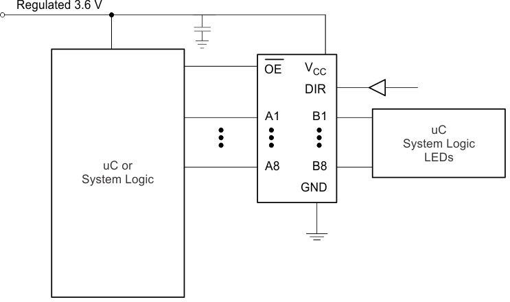
The SN74ALVC16245 device is a 16-bit bidirectional transceiver. This device can be used as two 8-bit transceivers or one 16-bit transceiver. It allows data transmission from the A bus to the B bus or from the B bus to the A bus, depending on the logic level at the direction-control (DIR) input. The output-enable (OE) input can be used to disable the device so that the buses are effectively isolated. This allows it to be used in multi-power systems and for down translation as well.
9.2 Typical Application
 Figure 7. Typical Application Schematic
9.2.1 Design Requirements
This device uses CMOS technology and has balanced output drive. Take care to avoid bus contention because it can drive currents that would exceed maximum limits. The high drive also creates fast edges into light loads; therefore, routing and load conditions must be considered to prevent ringing.
9.2.2 Detailed Design Procedure
- Recommended Input Conditions
- Rise time and fall time specs: See (Δt/ΔV) in Recommended Operating Conditions: VCCB at 3.3 V.
- Specified high and low levels: See (VIH and VIL) in Recommended Operating Conditions: VCCB at 3.3 V.
- Recommend Output Conditions
- Load currents should not exceed 50 mA per output and 100 mA total for the part.
- Outputs should not be pulled above VCC.
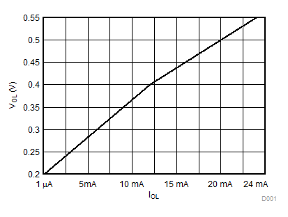
9.2.3 Application Curve
