ZHCSHV1A March 2018 – May 2018 SN65LVDS93B-Q1
PRODUCTION DATA.
6.6 Timing Requirements
| PARAMETER | MIN | MAX | UNIT | |
|---|---|---|---|---|
| Input clock period, tc | 7.4 | 100 | ns | |
| Input clock modulation | with modulation frequency 30 kHz | 8% | ||
| with modulation frequency 50 kHz | 6% | |||
| High-level input clock pulse width duration, tw | 0.4 tc | 0.6 tc | ns | |
| Input signal transition time, tt | 3 | ns | ||
| Data set up time, D0 through D27 before CLKIN (See Figure 4) | 2 | ns | ||
| Data hold time, D0 through D27 after CLKIN | 0.8 | ns | ||
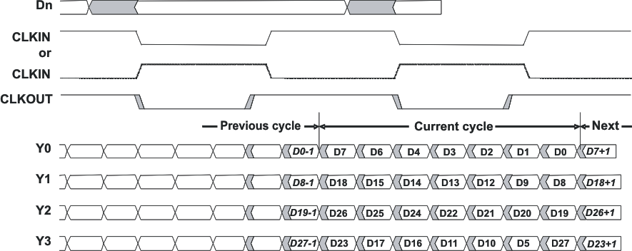
 Figure 1. Typical SN65LVDS93B-Q1 Load and Shift Sequences
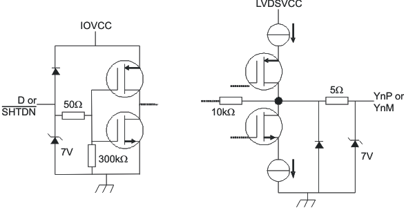
  Figure 2. Equivalent Input and Output Schematic Diagrams