ZHCS369A July   2011  – November 2015 SN65LVDS4

PRODUCTION DATA.  

  1. 特性
  2. 应用
  3. 说明
  4. 修订历史记录
  5. Pin Configuration and Functions
  6. Specifications
    1. 6.1 Absolute Maximum Ratings
    2. 6.2 ESD Ratings
    3. 6.3 Recommended Operating Conditions
    4. 6.4 Thermal Information
    5. 6.5 Receiver Electrical Characteristics: VCC = 2.5 V
    6. 6.6 Receiver Electrical Characteristics: VCC = 1.8 V
    7. 6.7 Receiver Switching Characteristics: VCC = 2.5 V
    8. 6.8 Receiver Switching Characteristics: VCC = 1.8 V
    9. 6.9 Typical Characteristics
  7. Parameter Measurement Information
  8. Detailed Description
    1. 8.1 Overview
    2. 8.2 Functional Block Diagram
    3. 8.3 Feature Description
      1. 8.3.1 Failsafe
        1. 8.3.1.1 R1 and R3 Calculation With VCC = 1.8 V
        2. 8.3.1.2 R1 and R3 Calculation With VCC = 2.5 V
    4. 8.4 Device Functional Modes
      1. 8.4.1 Maximum Input Voltage, VIN(max)
  9. Application and Implementation
    1. 9.1 Application Information
    2. 9.2 Typical Application
      1. 9.2.1 Design Requirements
      2. 9.2.2 Detailed Design Procedure
        1. 9.2.2.1 Receiver Bypass Capacitance
        2. 9.2.2.2 Receiver Input Voltage
        3. 9.2.2.3 Interconnecting Media
        4. 9.2.2.4 PCB Transmission Lines
        5. 9.2.2.5 Termination Resistor
      3. 9.2.3 Application Curves
  10. 10Power Supply Recommendations
  11. 11Layout
    1. 11.1 Layout Guidelines
      1. 11.1.1 Microstrip vs. Stripline Topologies
      2. 11.1.2 Dielectric Type and Board Construction
      3. 11.1.3 Recommended Stack Layout
      4. 11.1.4 Separation Between Traces
      5. 11.1.5 Crosstalk and Ground Bounce Minimization
      6. 11.1.6 Decoupling
    2. 11.2 Layout Example
  12. 12器件和文档支持
    1. 12.1 社区资源
    2. 12.2 商标
    3. 12.3 静电放电警告
    4. 12.4 Glossary
  13. 13机械、封装和可订购信息

封装选项

机械数据 (封装 | 引脚)
散热焊盘机械数据 (封装 | 引脚)
订购信息

Pin Configuration and Functions

RSE Package
10-Pin UQFN
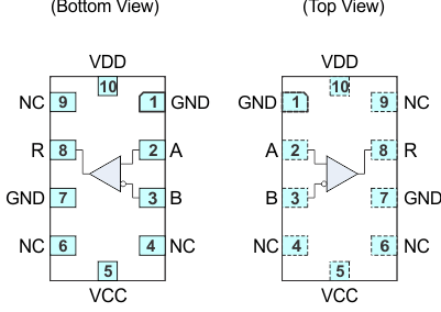
SN65LVDS4 PO_LLSE15.gif

Pin Functions

PIN I/O DESCRIPTION
NAME NO.
A 2 I LVDS input, positive
B 3 I LVDS input, negative
GND 1, 7 Ground
NC 4, 6, 9 No connect
R 8 O 1.8/2.5 LVCMOS/3.3 LVTTL output
VCC 5 Core supply voltage
VDD 10 Output drive voltage