SLLS236I October 1996 – June 2015 SN65LBC184 , SN75LBC184
PRODUCTION DATA.
- 1 Features
- 2 Applications
- 3 Description
- 4 Revision History
- 5 Pin Configuration and Functions
-
6 Specifications
- 6.1 Absolute Maximum Ratings
- 6.2 ESD Ratings
- 6.3 Recommended Operating Conditions
- 6.4 Thermal Information
- 6.5 Electrical Characteristics: Driver
- 6.6 Electrical Characteristics: Receiver
- 6.7 Driver Switching Characteristics
- 6.8 Receiver Switching Characteristics
- 6.9 Dissipation Ratings
- 6.10 Typical Characteristics
- 7 Parameter Measurement Information
- 8 Detailed Description
- 9 Application and Implementation
- 10Power Supply Recommendations
- 11Layout
- 12Device and Documentation Support
- 13Mechanical, Packaging, and Orderable Information
11 Layout
11.1 Layout Guidelines
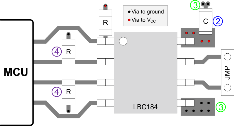
Because ESD transients have a wide frequency bandwidth from approximately 3 MHz to 3 GHz, high-frequency layout techniques must be applied during PCB design.
- Use VCC and ground planes to provide low inductance. High frequency currents follow the path of least inductance and not the path of least impedance.
- Apply 100-nF to 220-nF bypass capacitors as close as possible to the VCC pins of transceiver, UART, or controller ICs on the board.
- Use at least two vias for VCC and ground connections of bypass capacitors to minimize effective via-inductance.
- Use 1-kΩ to 10-kΩ pullup or pulldown resistors for enable lines to limit noise currents in these lines during transient events.
11.2 Layout Example
 Figure 21. Layout Schematic