SLLS236I October 1996 – June 2015 SN65LBC184 , SN75LBC184
PRODUCTION DATA.
- 1 Features
- 2 Applications
- 3 Description
- 4 Revision History
- 5 Pin Configuration and Functions
-
6 Specifications
- 6.1 Absolute Maximum Ratings
- 6.2 ESD Ratings
- 6.3 Recommended Operating Conditions
- 6.4 Thermal Information
- 6.5 Electrical Characteristics: Driver
- 6.6 Electrical Characteristics: Receiver
- 6.7 Driver Switching Characteristics
- 6.8 Receiver Switching Characteristics
- 6.9 Dissipation Ratings
- 6.10 Typical Characteristics
- 7 Parameter Measurement Information
- 8 Detailed Description
- 9 Application and Implementation
- 10Power Supply Recommendations
- 11Layout
- 12Device and Documentation Support
- 13Mechanical, Packaging, and Orderable Information
9 Application and Implementation
NOTE
Information in the following applications sections is not part of the TI component specification, and TI does not warrant its accuracy or completeness. TI’s customers are responsible for determining suitability of components for their purposes. Customers should validate and test their design implementation to confirm system functionality.
9.1 Application Information
The SN65LBC184 and SN75LBC184 devices are half-duplex, RS-485 transceivers commonly used for asynchronous data transmissions. The driver and receiver enable pins allow for the configuration of different operating modes.
 Figure 15. Half-Duplex Transceiver Configurations
- Using independent enable lines provides the most flexible control as it allows for the driver and the receiver to be turned on and off individually. While this configuration requires two control lines, it allows for selective listening into the bus traffic, whether the driver is transmitting data or not.
- Combining the enable signals simplifies the interface to the controller by forming a single direction-control signal. In this configuration, the transceiver operates as a driver when the direction-control line is high, and as a receiver when the direction-control line is low.
- Only one line is required when connecting the receiver-enable input to ground and controlling only the driver-enable input. In this configuration, a node not only receives the data from the bus, but also the data it sends and can verify that the correct data have been transmitted.
9.2 Typical Application
An RS-485 bus consists of multiple transceivers connected in parallel to a bus cable. To eliminate line reflections, each cable end is terminated with a termination resistor, RT, whose value matches the characteristic impedance, Z0, of the cable. This method, known as parallel termination, allows for higher data rates over a longer cable length.
 Figure 16. Typical RS-485 Network With Half-Duplex Transceivers
9.2.1 Design Requirements
RS-485 is a robust electrical standard suitable for long-distance networking that may be used in a wide range of applications with varying requirements, such as distance, data rate, and number of nodes.
9.2.1.1 Data Rate and Bus Length
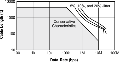
There is an inverse relationship between data rate and bus length, meaning the higher the data rate, the shorter the cable length; and conversely, the lower the data rate, the longer the cable may be without introducing data errors. While most RS-485 systems use data rates between 10 kbps and 100 kbps, some applications require data rates up to 250 kbps at distances of 4000 feet and longer. Longer distances are possible by allowing for small signal jitter of up to 5 or 10%.
 Figure 17. Cable Length vs Data Rate Characteristic
9.2.1.2 Stub Length
When connecting a node to the bus, the distance between the transceiver inputs and the cable trunk, known as the stub, should be as short as possible. Stubs present a nonterminated piece of bus line which can introduce reflections as the length of the stub increases. As a general guideline, the electrical length, or round-trip delay, of a stub should be less than one-tenth of the rise time of the driver, thus giving a maximum physical stub length as shown in Equation 1.
where
- tr is the 10/90 rise time of the driver
- v is the signal velocity of the cable or trace as a factor of c
- c is the speed of light (3 × 10⁸ m/s)
Per Equation 1, cable-stub lengths when using the SN65LBC184 driver must be not greater than 5.85 meters (19 feet) for a signal velocity of 78% and minimum driver output rise or fall time of 250 ns.
9.2.1.3 Bus Loading
The RS-485 standard specifies that a compliant driver must be able to driver 32 unit loads (UL), where 1 unit load represents a load impedance of approximately 12 kΩ. Because the SN65LBC184 is a 1/4 UL transceiver, it is possible to connect up to 128 receivers to the bus.
9.2.2 Detailed Design Procedure
9.2.2.1 SN65LBC184 Test Description
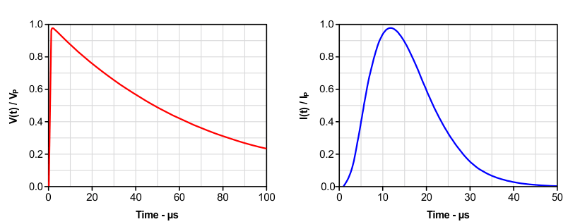
The SN65LBC184 is tested against the IEC 61000-4-5 recommended transient identified as the combination wave. The combination wave provides a 1.2-/50-μs open-circuit voltage waveform and a 8-/20-μs short-circuit current waveform shown in Figure 18. The testing is performed with a combination/hybrid pulse generator with an effective output impedance of 2 Ω. The setup for the overvoltage stress is shown in Figure 19 with all testing performed with power applied to the SN65LBC184 circuit.
 Figure 18. Open-Circuit Voltage and Short-Circuit Current Waveforms
The SN65LBC184 is tested and evaluated for both maximum (single pulse) as well as life test (multiple pulse) capabilities. The SN65LBC184 is evaluated against transients of both positive and negative polarity and all testing is performed with the worst-case transient polarity. Transient pulses are applied to the bus pins (A and B) across ground as shown in Figure 19.
 Figure 19. Overvoltage Stress Test Circuit
9.2.3 Application Curve
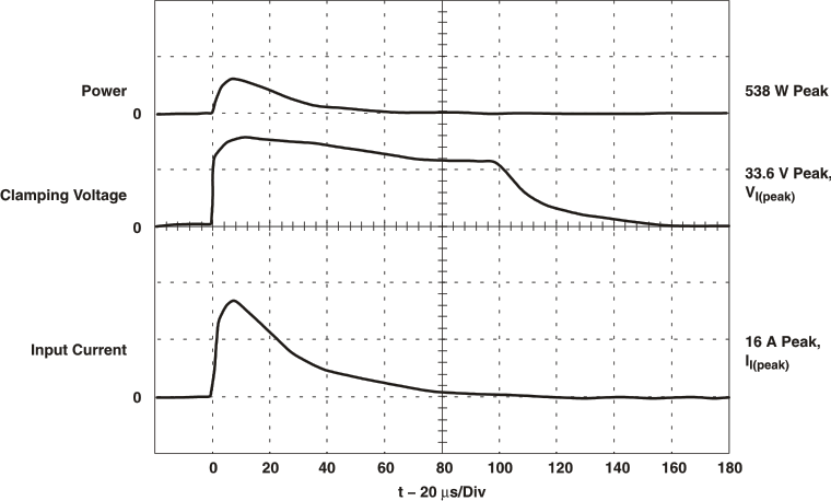
An example waveform as seen by the SN65LBC184 is shown in Figure 20. The bottom trace is current, the middle trace shows the clamping voltage of the device and the top trace is power as calculated from the voltage and current waveforms. This example shows a peak clamping voltage of 33.6 V and peak current of 16 A, thus yielding an absorbed peak power of 538 W.
 Figure 20. Typical Surge Waveform Measured at Pins 5 and 7