SLAS638A January 2009 – October 2015 SN65HVS885
PRODUCTION DATA.
- 1 Features
- 2 Applications
- 3 Description
- 4 Revision History
- 5 Pin Configuration and Functions
- 6 Specifications
- 7 Parameter Measurement Information
- 8 Detailed Description
- 9 Application and Implementation
- 10Power Supply Recommendations
- 11Layout
- 12Device and Documentation Support
- 13Mechanical, Packaging, and Orderable Information
封装选项
机械数据 (封装 | 引脚)
- PWP|28
散热焊盘机械数据 (封装 | 引脚)
- PWP|28
订购信息
8 Detailed Description
8.1 Overview
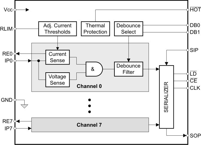
The SN65HVS885 is an 8 channel, digital input serializer which operates from a 5 V supply and accepts digital inputs of up to 34 V on the 8 channels (IP0-IP7). The device provides a serially shifted digital output with reduced voltage ranges of 0-5 V for applications in industrial and building automation systems. The SN65HVS885 meets JEDEC standards for ESD protection (refer to ESD Ratings), and is SPI compatible for interfacing with standard microcontrollers. The serializer operates in 2 fundamental modes: Load Mode and Shift mode. In Load mode, information from the field inputs is allowed to latch into the shift register. In Shift mode, the information stored in the parallel shift register can be serially shifted to the serial output (SOP). A detailed description of the functional modes is available in the Device Functional Modes section.
8.2 Functional Block Diagram

8.3 Feature Description
8.3.1 Digital Inputs
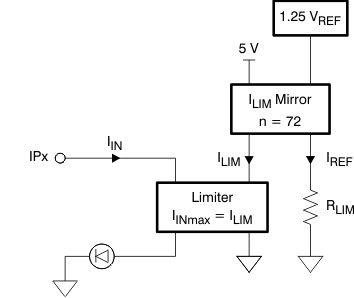
 Figure 10. Digital Input Stage
Each digital input operates as a controlled current sink limiting the input current to a maximum value of ILIM. The current limit is derived from the reference current via ILIM = n × IREF, and IREF is determined by IREF = VREF/RLIM. Thus, changing the current limit requires the change of RLIM to a different value via: RLIM = n × VREF/ILIM.
Inserting the actual values for n and VREF gives: RLIM = 90 V / ILIM.
While the device is specified for a current limit of 3.6 mA, (via RLIM = 25 kΩ), it is easy to lower the current limit to further reduce the power consumption. For example, for a current limit of 2.5 mA simply calculate:

8.3.2 Debounce Filter
The HVS885 applies a simple analog/digital filtering technique to remove unintended signal transitions due to contact bounce or other mechanical effects. Any new input (either low or high) must be present for the duration of the selected debounce time to be latched into the shift register as a valid state.
The logic signal levels at the control inputs, DB0 and DB1 of the internal Debounce-Select logic determine the different debounce times listed in the following truth table.
Table 1. Debounce Times
| DB1 | DB0 | FUNCTION |
|---|---|---|
| Open | Open | 3 ms delay |
| Open | GND | 1 ms delay |
| GND | Open | 0 ms delay (Filter bypassed) |
| GND | GND | Reserved |
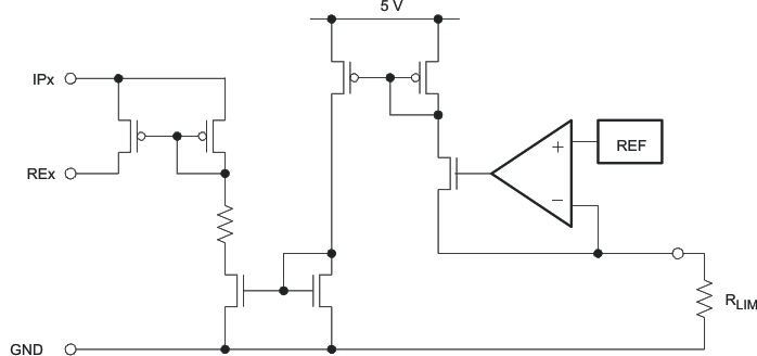
 Figure 11. Equivalent Input Diagram
8.3.3 Shift Register
The conversion from parallel input to serial output data is performed by an eight-channel, parallel-in serial-out shift register. Parallel-in access is provided by the internal inputs, PIP0–PIP7, that are enabled by a low level at the load input (LD). When clocked, the latched input data shift towards the serial output (SOP). The shift register also provides a clock-enable function.
Clocking is accomplished by a low-to-high transition of the clock (CLK) input while LD is held high and the clock enable (CE) input is held low. Parallel loading is inhibited when LD is held high. The parallel inputs to the register are enabled while LD is low independently of the levels of the CLK, CE, or serial (SIP) inputs.
 Figure 12. Shift Register Logic Structure
Table 2. Function Table
| INPUTS | FUNCTION | ||
|---|---|---|---|
| LD | CLK | CE | |
| L | X | X | Parallel load |
| H | X | H | No change |
| H | ↑ | L | Shift(1) |
8.3.4 Temperature Sensor
An on-chip temperature sensor monitors the device temperature and signals a fault condition if the temperature exceeds a first trip point at 150°C by pulling the HOT output low. If the junction temperature continues to rise, passing a second trip point at 170 °C, all device outputs assume high impedance state.
A special condition occurs when the chip temperature exceeds the second temperature trip point due to an output short; the HOT output buffer becomes high impedance, thus separating the buffer from the external circuitry. An internal 100-kΩ pulldown resistor, connecting the HOT-pin to ground, is used as a "cooling down" resistor, which continues to provide a logic low level to the external circuitry.
8.4 Device Functional Modes
The 2 functional modes of operation are Load mode and Shift mode. Load mode enables information from the field inputs to latch into the shift register. To enter load mode, the LD pin must be held low, and the device will remain in load mode regardless of the CLK, CE, or serial (SIP) input levels. A high level at the LD pin switches the device into Shift mode. When the device is in Shift mode, a low level at the CE pin will cause the data stored in the parallel shift register to be serially shifted to the serial output (SOP) on the rising edge of CLK. A high level at the CE pin inhibits the serial shifting, which is demonstrated in Figure 17. After 8 consecutive CLK pulses, the serial output (SOP) will remain at the level of the serial input (SIP) which is internally pulled to logic high. A logic high at the CE pin is required to signify the end of the serial data output. In the case of a daisy chained configuration, the serial output (SOP) of the SN65HVS885 can be connected to the serial input (SIP) of a following device, and additional clock pulses are required to shift the additional data out of the chain. The number of consecutive clock pulses will equal 8 times the number of devices in the chain. See Figure 18 for an example of a cascaded chain of 4x SN65HVS885.