ZHCSJZ5 June   2019 SN65HVDA1040B-Q1

PRODUCTION DATA.  

  1. 特性
  2. 应用
  3. 说明
    1.     方框图
  4. 修订历史记录
  5. Pin Configuration and Functions
    1.     Pin Functions
  6. Specifications
    1. 6.1 Absolute Maximum Ratings
    2. 6.2 ESD Ratings
    3. 6.3 Recommended Operating Conditions
    4. 6.4 Thermal Information
    5. 6.5 Electrical Characteristics
    6. 6.6 Power Dissipation Characteristics
    7. 6.7 Switching Characteristics
    8. 6.8 Typical Characteristics
  7. Parameter Measurement Information
  8. Detailed Description
    1. 8.1 Overview
    2. 8.2 Functional Block Diagram
    3. 8.3 Feature Description
      1. 8.3.1 Operating Modes
        1. 8.3.1.1 Bus States by Mode
        2. 8.3.1.2 Normal Mode
        3. 8.3.1.3 Standby Mode and RXD Wake-Up Request
      2. 8.3.2 Protection Features
        1. 8.3.2.1 TXD Dominant State Time-Out
        2. 8.3.2.2 Thermal Shutdown
        3. 8.3.2.3 Undervoltage Lockout and Unpowered Device
    4. 8.4 Device Functional Modes
  9. Application and Implementation
    1. 9.1 Application Information
      1. 9.1.1 Using With 3.3-V Microcontrollers
      2. 9.1.2 Using SPLIT With Split Termination
    2. 9.2 Typical Application
      1. 9.2.1 Design Requirements
        1. 9.2.1.1 Bus Loading, Length, and Number of Nodes
        2. 9.2.1.2 CAN Termination
        3. 9.2.1.3 Loop Propagation Delay
      2. 9.2.2 Detailed Design Procedure
        1. 9.2.2.1 Transient Voltage Suppresser (TVS) Diodes
      3. 9.2.3 Application Curves
  10. 10Power Supply Recommendations
  11. 11Layout
    1. 11.1 Layout Guidelines
    2. 11.2 Layout Example
    3. 11.3 ESD Protection
  12. 12器件和文档支持
    1. 12.1 文档支持
      1. 12.1.1 相关文档
    2. 12.2 接收文档更新通知
    3. 12.3 社区资源
    4. 12.4 商标
    5. 12.5 静电放电警告
    6. 12.6 Glossary
  13. 13机械、封装和可订购信息

封装选项

机械数据 (封装 | 引脚)
散热焊盘机械数据 (封装 | 引脚)
订购信息

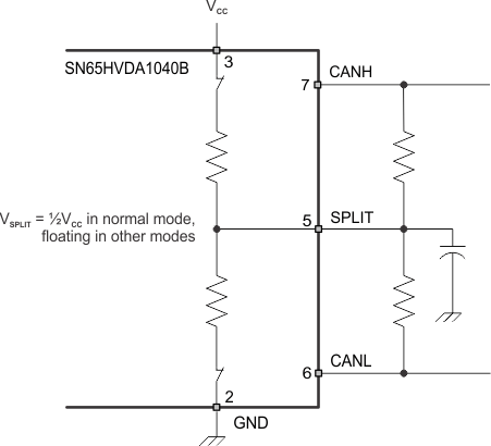
Using SPLIT With Split Termination

The SPLIT pin voltage output provides 0.5 × VCC in normal mode. The circuit may be used by the application to stabilized the common-mode voltage of the bus by connecting it to the center tap of split termination for the CAN network (see Figure 19 and Figure 20). This pin provides a stabilizing recessive voltage drive to offset leakage currents of unpowered transceivers or other bias imbalances that might bring the network common-mode voltage away from 0.5 × VCC. Using this feature in a CAN network improves electromagnetic emissions behavior of the network by eliminating fluctuations in the bus common-mode voltage levels at the start of message transmissions.
SN65HVDA1040B-Q1 split_pin_stabil_llsef2.gifFigure 19. Split Pin Stabilization Circuitry and Application