ZHCSJZ5 June   2019 SN65HVDA1040B-Q1

PRODUCTION DATA.  

  1. 特性
  2. 应用
  3. 说明
    1.     方框图
  4. 修订历史记录
  5. Pin Configuration and Functions
    1.     Pin Functions
  6. Specifications
    1. 6.1 Absolute Maximum Ratings
    2. 6.2 ESD Ratings
    3. 6.3 Recommended Operating Conditions
    4. 6.4 Thermal Information
    5. 6.5 Electrical Characteristics
    6. 6.6 Power Dissipation Characteristics
    7. 6.7 Switching Characteristics
    8. 6.8 Typical Characteristics
  7. Parameter Measurement Information
  8. Detailed Description
    1. 8.1 Overview
    2. 8.2 Functional Block Diagram
    3. 8.3 Feature Description
      1. 8.3.1 Operating Modes
        1. 8.3.1.1 Bus States by Mode
        2. 8.3.1.2 Normal Mode
        3. 8.3.1.3 Standby Mode and RXD Wake-Up Request
      2. 8.3.2 Protection Features
        1. 8.3.2.1 TXD Dominant State Time-Out
        2. 8.3.2.2 Thermal Shutdown
        3. 8.3.2.3 Undervoltage Lockout and Unpowered Device
    4. 8.4 Device Functional Modes
  9. Application and Implementation
    1. 9.1 Application Information
      1. 9.1.1 Using With 3.3-V Microcontrollers
      2. 9.1.2 Using SPLIT With Split Termination
    2. 9.2 Typical Application
      1. 9.2.1 Design Requirements
        1. 9.2.1.1 Bus Loading, Length, and Number of Nodes
        2. 9.2.1.2 CAN Termination
        3. 9.2.1.3 Loop Propagation Delay
      2. 9.2.2 Detailed Design Procedure
        1. 9.2.2.1 Transient Voltage Suppresser (TVS) Diodes
      3. 9.2.3 Application Curves
  10. 10Power Supply Recommendations
  11. 11Layout
    1. 11.1 Layout Guidelines
    2. 11.2 Layout Example
    3. 11.3 ESD Protection
  12. 12器件和文档支持
    1. 12.1 文档支持
      1. 12.1.1 相关文档
    2. 12.2 接收文档更新通知
    3. 12.3 社区资源
    4. 12.4 商标
    5. 12.5 静电放电警告
    6. 12.6 Glossary
  13. 13机械、封装和可订购信息

封装选项

机械数据 (封装 | 引脚)
散热焊盘机械数据 (封装 | 引脚)
订购信息

Bus States by Mode

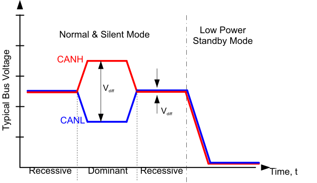
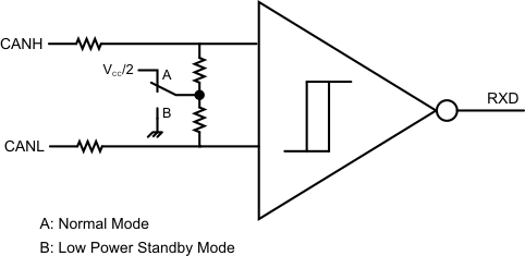
The CAN bus has three valid states during powered operation depending on the mode of the device. In normal mode the bus may be dominant (logic low) where the bus lines are driven differentially apart or recessive (logic high) where the bus lines are biased to VCC/2 through the high-ohmic internal input resistors RIN of the receiver. The third state is low-power standby mode where the bus lines is biased to GND through the high-ohmic internal input resistors RIN of the receiver.
SN65HVDA1040B-Q1 bus_states_physical_bit_lls804.gif
Figure 16. Bus States (Physical Bit Representation)
SN65HVDA1040B-Q1 simplified_common_mode_bias_lls804.gif
Figure 17. Simplified Common-Mode Bias and Receiver Implementation