ZHCS823H March   2012  – March 2019 SN65HVD72 , SN65HVD75 , SN65HVD78

UNLESS OTHERWISE NOTED, this document contains PRODUCTION DATA.  

  1. 特性
  2. 应用
  3. 说明
    1.     Device Images
      1.      典型应用图
  4. 修订历史记录
  5. Device Comparison Table
  6. Pin Configuration and Functions
    1.     Pin Functions
  7. Specifications
    1. 7.1  Absolute Maximum Ratings
    2. 7.2  ESD Ratings
    3. 7.3  Recommended Operating Conditions
    4. 7.4  Thermal Information
    5. 7.5  Electrical Characteristics
    6. 7.6  Power Dissipation
    7. 7.7  Switching Characteristics: 250 kbps Device (SN65HVD72) Bit Time ≥ 4 µs
    8. 7.8  Switching Characteristics: 20 Mbps Device (SN65HVD75) Bit Time ≥50 ns
    9. 7.9  Switching Characteristics: 50 Mbps Device (SN65HVD78) Bit Time ≥20 ns
    10. 7.10 Typical Characteristics
  8. Parameter Measurement Information
  9. Detailed Description
    1. 9.1 Overview
    2. 9.2 Functional Block Diagram
    3. 9.3 Feature Description
    4. 9.4 Device Functional Modes
  10. 10Application and Implementation
    1. 10.1 Application Information
    2. 10.2 Typical Application
      1. 10.2.1 Design Requirements
        1. 10.2.1.1 Data Rate and Bus Length
        2. 10.2.1.2 Stub Length
        3. 10.2.1.3 Bus Loading
        4. 10.2.1.4 Receiver Failsafe
        5. 10.2.1.5 Transient Protection
      2. 10.2.2 Detailed Design Procedure
        1. 10.2.2.1 External Transient Protection
        2. 10.2.2.2 Isolated Bus Node Design
      3. 10.2.3 Application Curves
  11. 11Power Supply Recommendations
  12. 12Layout
    1. 12.1 Layout Guidelines
    2. 12.2 Layout Example
  13. 13器件和文档支持
    1. 13.1 器件支持
      1. 13.1.1 第三方产品免责声明
    2. 13.2 文档支持
      1. 13.2.1 相关文档
    3. 13.3 相关链接
    4. 13.4 社区资源
    5. 13.5 商标
    6. 13.6 静电放电警告
    7. 13.7 术语表
  14. 14机械、封装和可订购信息

封装选项

机械数据 (封装 | 引脚)
散热焊盘机械数据 (封装 | 引脚)
订购信息

Typical Characteristics

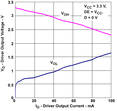
SN65HVD72 SN65HVD75 SN65HVD78 drvo_io_llsE11.gifFigure 1. Driver Output Voltage vs Driver Output Current
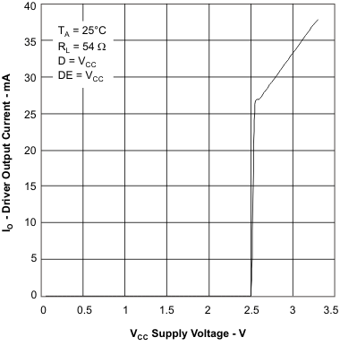
SN65HVD72 SN65HVD75 SN65HVD78 io_vcc_4_llsE11.gifFigure 3. Driver Output Current vs Supply Voltage
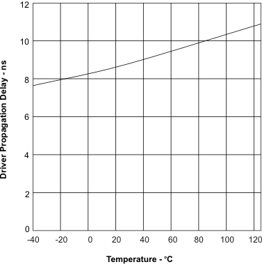
SN65HVD72 SN65HVD75 SN65HVD78 Driver_prop_delay_HVD78_llsE11.gifFigure 5. SN65HVD78 Driver Propagation Delay vs Temperature
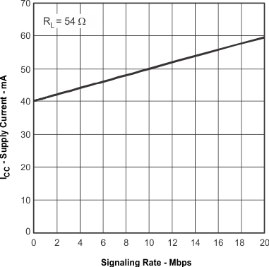
SN65HVD72 SN65HVD75 SN65HVD78 sup_cur_HVD75_llsE11.gifFigure 7. SN65HVD75 Supply Current vs Signal Rate
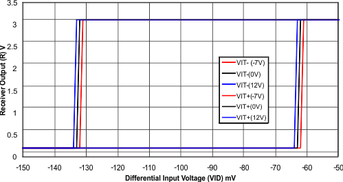
SN65HVD72 SN65HVD75 SN65HVD78 rec_outin_llsE11.gifFigure 9. Receiver Output vs Input
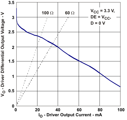
SN65HVD72 SN65HVD75 SN65HVD78 difvo_io_llsE11.gifFigure 2. Driver Differential Output Voltage vs Driver Output Current
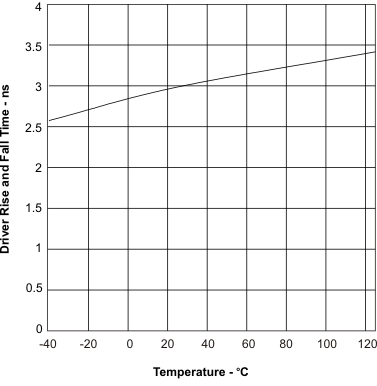
SN65HVD72 SN65HVD75 SN65HVD78 Driver_rise_fall_HVD78_llsE11.gifFigure 4. SN65HVD78 Driver Rise or Fall Time vs Temperature
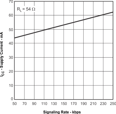
SN65HVD72 SN65HVD75 SN65HVD78 sup_cur_HVD72_llsE11.gifFigure 6. SN65HVD72 Supply Current vs Signal Rate
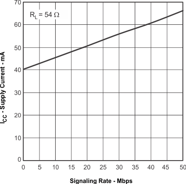
SN65HVD72 SN65HVD75 SN65HVD78 sup_cur_HVD78_llsE11.gifFigure 8. SN65HVD78 Supply Current vs Signal Rate