ZHCSAT9I september   2012  – october 2020 SN65DSI83

PRODUCTION DATA  

  1.   1
  2. 特性
  3. 应用
  4. 说明
  5. Revision History
  6. Pin Configuration and Functions
  7. Specifications
    1. 6.1 Absolute Maximum Ratings #GUID-BDB96F65-5C5F-4805-AA4B-B71B15ADA38F/SLLSEB91839
    2. 6.2 ESD Ratings
    3. 6.3 Recommended Operating Conditions
    4. 6.4 Thermal Information
    5. 6.5 Electrical Characteristics
    6. 6.6 Timing Requirements
    7. 6.7 Switching Characteristics
  8. Detailed Description
    1. 7.1 Overview
    2. 7.2 Functional Block Diagram
    3. 7.3 Feature Description
      1. 7.3.1 Clock Configurations and Multipliers
      2. 7.3.2 ULPS
      3. 7.3.3 LVDS Pattern Generation
    4. 7.4 Device Functional Modes
      1. 7.4.1 Reset Implementation
      2. 7.4.2 Initialization Sequence
      3. 7.4.3 LVDS Output Formats
      4. 7.4.4 DSI Lane Merging
      5. 7.4.5 DSI Pixel Stream Packets
      6. 7.4.6 DSI Video Transmission Specifications
    5. 7.5 Programming
      1. 7.5.1 Local I2C Interface Overview
    6. 7.6 Register Maps
      1. 7.6.1 Control and Status Registers Overview
  9. Application and Implementation
    1. 8.1 Application Information
      1. 8.1.1 Video STOP and Restart Sequence
      2. 8.1.2 Reverse LVDS Pin Order Option
      3. 8.1.3 IRQ Usage
    2. 8.2 Typical Application
      1. 8.2.1 Design Requirements
      2. 8.2.2 Detailed Design Procedure
        1. 8.2.2.1 Example Script
      3. 8.2.3 Application Curve
  10. Power Supply Recommendations
    1. 9.1 VCC Power Supply
    2. 9.2 VCORE Power Supply
  11. 10Layout
    1. 10.1 Layout Guidelines
      1. 10.1.1 Package Specific
      2. 10.1.2 Differential Pairs
      3. 10.1.3 Ground
    2. 10.2 Layout Example
  12. 11Device and Documentation Support
    1. 11.1 Receiving Notification of Documentation Updates
    2. 11.2 Community Resources
    3. 11.3 Trademarks
  13.   Mechanical, Packaging, and Orderable Information

封装选项

机械数据 (封装 | 引脚)
散热焊盘机械数据 (封装 | 引脚)
订购信息

Typical Application

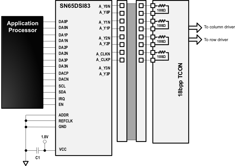
Figure 8-1 shows a typical application using the SN65DSI83 device for a single channel DSI receiver to interface a single-channel DSI application processor to an LVDS single-link 18 bit-per-pixel panel supporting 1280 × 800 WXGA resolutions at 60 frames per second.
GUID-32965D92-8C4D-4456-B042-D0824FF16964-low.gifFigure 8-1 Typical WXGA 18-bpp Panel Application