ZHCSAT9I september 2012 – october 2020 SN65DSI83
PRODUCTION DATA
- 1
- 1 特性
- 2 应用
- 3 说明
- 4 Revision History
- 5 Pin Configuration and Functions
- 6 Specifications
- 7 Detailed Description
- 8 Application and Implementation
- 9 Power Supply Recommendations
- 10Layout
- 11Device and Documentation Support
- Mechanical, Packaging, and Orderable Information
7.4.1 Reset Implementation
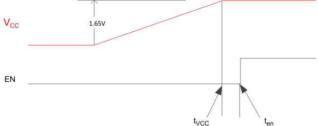
When EN is deasserted (low), the SN65DSI83 device is in shutdown or reset state. In this state, CMOS inputs are ignored, the MIPI D-PHY inputs are disabled and outputs are high impedance. It is critical to transition the EN input from a low level to a high level after the VCC supply has reached the minimum operating voltage, as shown in Figure 7-1. This is achieved by a control signal to the EN input, or by an external capacitor connected between EN and GND.
 Figure 7-1 Cold Start VCC Ramp up to EN
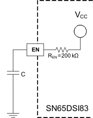
When implementing the external capacitor, the size of the external capacitor depends on the power-up ramp of the VCC supply, where a slower ramp-up results in a larger value external capacitor. See the latest reference schematic for the SN65DSI83 device and, or consider approximately 200-nF capacitor as a reasonable first estimate for the size of the external capacitor.
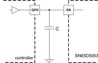
Both EN implementations are shown in Figure 7-2 and Figure 7-3.
 Figure 7-2 External Capacitor Controlled EN
 Figure 7-3 EN Input from Active Controller
When the SN65DSI83 is reset while VCC is high, the EN pin must be held low for at least 10 ms before being asserted high as described in Table 7-2 to be sure that the device is properly reset. The DSI CLK lane MUST be in HS and the DSI data lanes MUST be driven to LP11 while the device is in reset before the EN pin is asserted per the timing described in Table 7-2.