ZHCSRC8B April   1998  – January 2023 SN65ALS1176

PRODUCTION DATA  

  1. 特性
  2. 应用
  3. 说明
  4. Revision History
  5. Pin Configuration and Functions
  6. Specifications
    1. 6.1 Absolute Maximum Ratings
    2. 6.2 Recommended Operating Conditions
    3. 6.3 Thermal Information
    4. 6.4 Electrical Characteristics - Driver
    5. 6.5 Switching Characteristics - Driver
    6. 6.6 Symbol Equivalents
    7. 6.7 Electrical Characteristics - Receiver
    8. 6.8 Switching Characteristics - Receiver
  7. Parameter Measurement Information
  8. Detailed Description
    1. 8.1 Functional Block Diagram
    2. 8.2 Device Functional Modes
  9. Application and Implementation
    1. 9.1 Application Information
      1. 9.1.1 Typical Application
  10. 10Device and Documentation Support
    1. 10.1 Documentation Support
      1. 10.1.1 Related Documentation
    2. 10.2 接收文档更新通知
    3. 10.3 支持资源
    4. 10.4 Trademarks
    5. 10.5 静电放电警告
    6. 10.6 术语表
  11. 11Mechanical, Packaging, and Orderable Information

封装选项

请参考 PDF 数据表获取器件具体的封装图。

机械数据 (封装 | 引脚)
  • D|8
散热焊盘机械数据 (封装 | 引脚)
订购信息

Pin Configuration and Functions

GUID-20220712-SS0I-HKF2-KGP7-4SZXGKPLV0TS-low.png
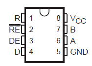
The D package is available taped and reeled. Add the suffix R to the device type (for example, SN65ALS1176DR).
Figure 5-1 D Package (Top View)
Table 5-1 Pin Functions
NONameTypeDescription
1R

O

Receive data output
2RE

I

Receiver enable, active low
3DE

I

Driver enable, active high
4D

I

Driver data input
5GND

GND

Local device ground
6A

I/O

Driver output or receiver input (complementary to B)
7B

I/O

Driver output or receiver input (complementary to A)
8VCC

SUPPLY

4.75-V to 5.25-V supply