SGUS034F February 2001 – June 2015 SMJ320VC33
PRODUCTION DATA.
- 1 Features
- 2 Description
- 3 Revision History
- 4 Description (continued)
- 5 Pin Configuration and Functions
-
6 Specifications
- 6.1 Absolute Maximum Ratings
- 6.2 Recommended Operating Conditions
- 6.3 Electrical Characteristics
- 6.4 Phase-Locked Loop Characteristics Using EXTCLK or On-Chip Crystal Oscillator Timing Requirements
- 6.5 Circuit Parameters for On-Chip Crystal Oscillator Timing Requirements
- 6.6 Timing Requirements for EXTCLK, All Modes
- 6.7 Timing Requirements for Memory Read/Write for STRB
- 6.8 Timing Requirements for XF0 and XF1 when Executing LDFI or LDII
- 6.9 Timing Requirements for XF0 and XF1 when Executing SIGI
- 6.10 Timing Requirements for Changing XFx from Output to Input Mode
- 6.11 Timing Requirements for RESET
- 6.12 Timing Requirements for INT3 to INT0 Response
- 6.13 Timing Requirements for Serial Port
- 6.14 Timing Requirements for HOLD/HOLDA
- 6.15 Timing Requirements for Peripheral Pin General-Purpose I/O
- 6.16 Timing Requirements for Timer Pin
- 6.17 Timing Requirements for IEEE-1149.1 Test Access Port
- 6.18 Switching Characteristics for EXTCLK, All Modes
- 6.19 Switching Characteristics for Memory Read/Write for STRB
- 6.20 Switching Characteristics for XF0 and XF1 when Executing LDFI or LDII
- 6.21 Switching Characteristics for XF0 when Executing STFI or STII
- 6.22 Switching Characteristics for XF0 and XF1 when Executing SIGI
- 6.23 Switching Characteristics for Loading when XF is Configured as an Output
- 6.24 Switching Characteristics for Changing XFx from Output to Input Mode
- 6.25 Switching Characteristics for Changing XFx from an Input to an Output
- 6.26 Switching Characteristics for RESET
- 6.27 Switching Characteristics for IACK
- 6.28 Switching Characteristics for Serial Port
- 6.29 Switching Characteristics for HOLD/HOLDA
- 6.30 Switching Characteristics for Peripheral Pin General-Purpose I/O
- 6.31 Switching Characteristics for Timer Pin
- 6.32 Switching Characteristics for SHZ
- 7 Parameter Measurement Information
-
8 Detailed Description
- 8.1 Functional Block Diagram
- 8.2
Feature Description
- 8.2.1 JTAG Scan-Based Emulation Logic
- 8.2.2 Clock Generator
- 8.2.3 PLL and Clock Oscillator Control
- 8.2.4 PLL Isolation
- 8.2.5 Clock and PLL Considerations on Initialization
- 8.2.6 EDGEMODE
- 8.2.7 Reset Operation
- 8.2.8 PAGE0 to PAGE3 Select Lines
- 8.2.9 Using External Logic With the READY Pin
- 8.2.10 Posted Writes
- 8.2.11 Data Bus I/O Buffer
- 8.2.12 Bootloader Operation
- 8.2.13 JTAG Emulation
- 8.2.14 Designing a Target System Emulator Connector (14-Pin Header)
- 8.2.15 JTAG Emulator Cable Pod Logic
- 8.2.16 Reset Timing
- 8.2.17 Interrupt Response TIming
- 8.2.18 Interrupt-Acknowledge Timing
- 8.2.19 Data-Rate Timing Modes
- 8.2.20 HOLD Timing
- 8.2.21 General-Purpose I/O Timing
- 8.2.22 Peripheral Pin I/O Timing
- 8.2.23 Timer Pin Timing
- 8.3 Register Maps
- 9 Power Supply Recommendations
- 10Device and Documentation Support
- 11Mechanical, Packaging, and Orderable Information
7 Parameter Measurement Information
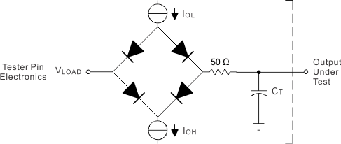
WHERE:
- IOL = 4 mA (all outputs) for dc levels test.
- IO and IOH are adjusted during ac timing analysis to achieve an ac termination of 50 Ω
- VLOAD = DVDD / 2
- CT = 40-pF typical load-circuit capacitance
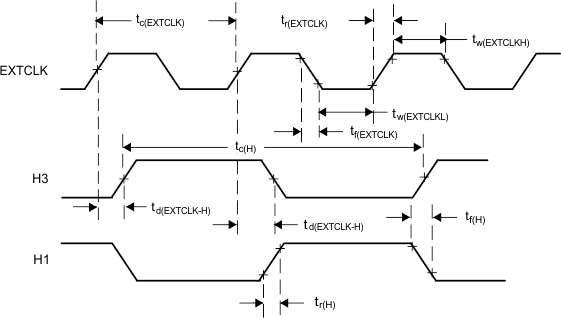 Figure 3. Divide-by-Two Mode
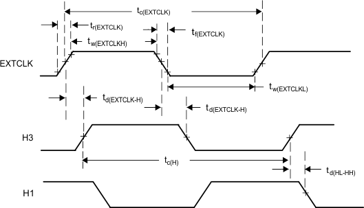
EXTCLK is held low.
Figure 4. Divide-by-One Mode
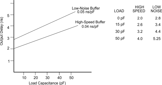
This figure shows output load characteristics for high-speed and low-speed (low-noise) output buffers. High-speed buffers are used on A0 to A23, PAGE0 to PAGE3, H1, H3, STRB, and R/W. All other outputs use the low-speed, (low-noise) output buffer.
CLmax = 30 pF
Figure 5. Output Load Characteristics, Buffer Only
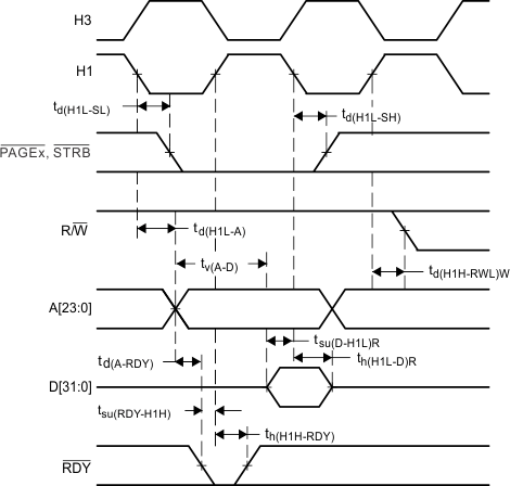
STRB remains low during back-to-back read operations.
Figure 6. Timing for Memory (STRB = 0 and PAGEx = 0) Read
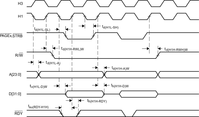 Figure 7. Timing for Memory (STRB = 0 and PAGEx = 0) Write
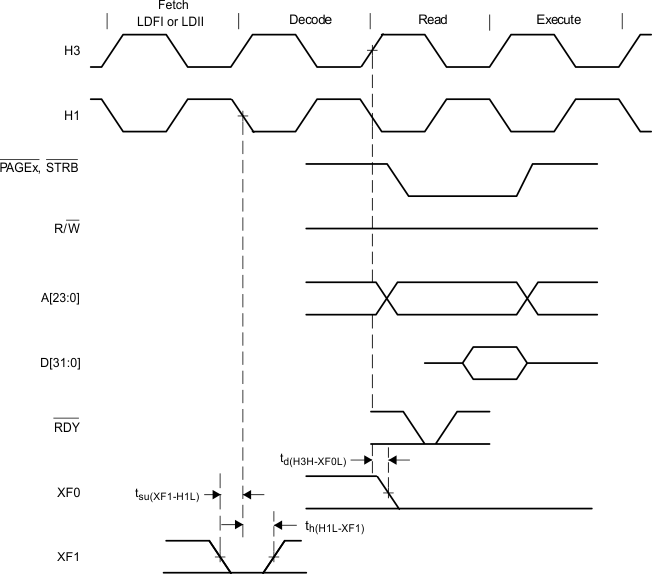 Figure 8. Timing for XF0 and XF1 When Executing LDFI or LDII
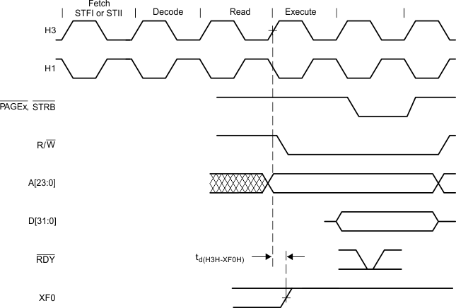 Figure 9. Timing for XF0 When Executing an STFI or STII
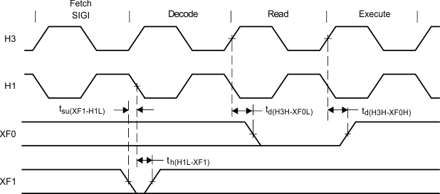 Figure 10. Timing for XF0 and XF1 When Executing SIGI
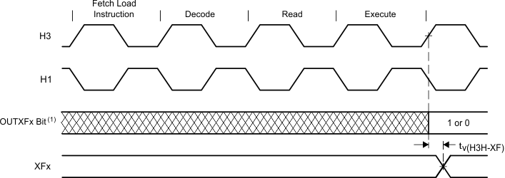
- OUTXFx represents either bit 2 or 6 of the IOF register
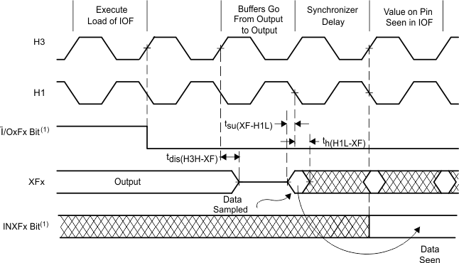
- I/OxFx represents either bit 1 or bit 5 of the IOF register, and INXFx represents either bit 3 or bit 7 of the IOF register.
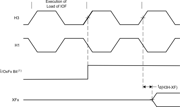
- I/OxFx represents either bit 1 or bit 5 of the IOF register.
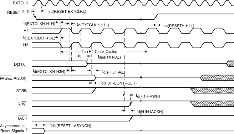
- Clock circuit is configured in C31-compatible divide-by-2 mode. If configured for x1 mode, EXTCLK directly drives H3.
- Asynchronous reset signals include XF0/1, CLKX0, DX0, FSX0, CLKR0, DR0, FSR0, and TCLK0/1.
- RESET is a synchronous input that can be asserted at any point during a clock cycle. If the specified timings are met, the exact sequence shown occurs; otherwise, an additional delay of one clock cycle is possible.
In microprocessor mode, the reset vector is fetched twice, with seven software wait states each time. In microcomputer mode, the reset vector is fetched twice, with no software wait states.
The address and PAGE3 to PAGE0 outputs are placed in a high-impedance state during reset requiring a nominal 10- to 22-kΩ pullup. If not, undesirable spurious reads can occur when these outputs are not driven.
Figure 14. RESET Timing
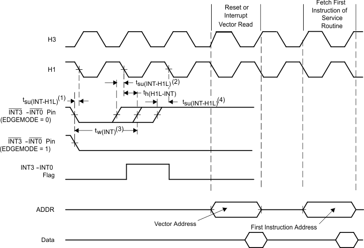
- Falling edge of H1 just detects INTx falling edge.
- Falling edge of H1 detects second INTx low, however flag clear takes precedence.
- Nominal width
- Falling edge of H1 misses previous INTx low as INTx rises.
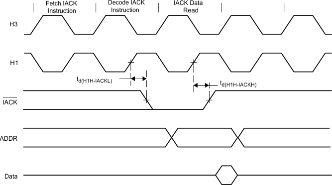 Figure 16. Interrupt Acknowledge (IACK) Timing
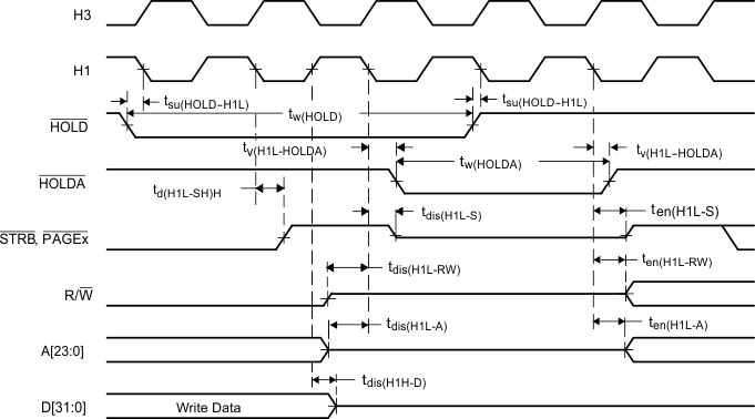
HOLDA goes low in response to HOLD going low and continues to remain low until one H1 cycle after HOLD goes back high.
Figure 17. Timing for HOLD/HOLDA (After Write)
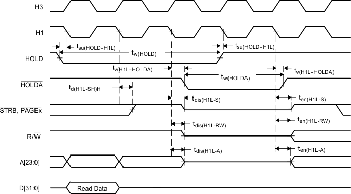
HOLDA goes low in response to HOLD going low and continues to remain low until one H1 cycle after HOLD goes back high.
Figure 18. Timing for HOLD/HOLDA (After Read)
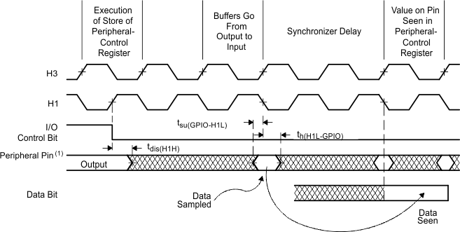
- Peripheral pins include CLKX0, CLKR0, DX0, DR0, FSX0, FSR0, and TCLK0/1.
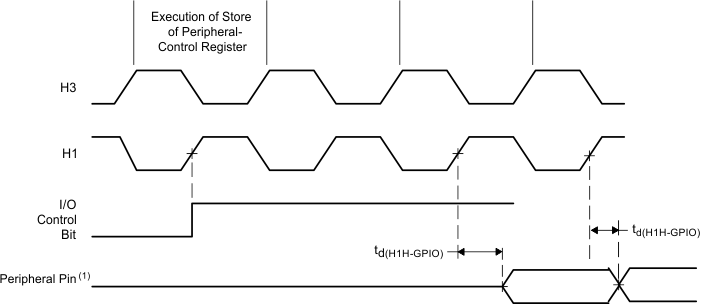
- Peripheral pins include CLKX0, CLKR0, DX0, DR0, FSX0, FSR0, and TCLK0/1.
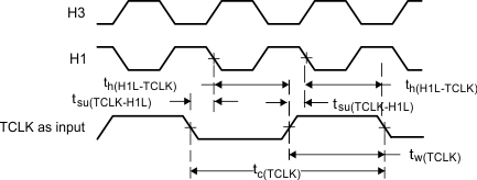 Figure 21. Timer Pin Timing, Input
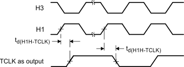 Figure 22. Timer Pin Timing, Output

Enabling SHZ destroys SMx320VC33 register and memory contents. Assert SHZ = 1 and reset the SMx320VC33 to restore it to a known condition.
Figure 23. Timing for SHZ
 Figure 24. IEEE-1149.1 Test Access Port Timings
