SBVS033C June 2002 – June 2016 REF2912 , REF2920 , REF2925 , REF2930 , REF2933 , REF2940
PRODUCTION DATA.
- 1 Features
- 2 Applications
- 3 Description
- 4 Revision History
- 5 Device Comparison Table
- 6 Pin Configuration and Functions
- 7 Specifications
- 8 Detailed Description
- 9 Application and Implementation
- 10Power Supply Recommendations
- 11Layout
- 12Device and Documentation Support
- 13Mechanical, Packaging, and Orderable Information
9 Application and Implementation
NOTE
Information in the following applications sections is not part of the TI component specification, and TI does not warrant its accuracy or completeness. TI’s customers are responsible for determining suitability of components for their purposes. Customers should validate and test their design implementation to confirm system functionality.
9.1 Application Information
For normal operation, the REF29xx does not require a capacitor on the output. If a capacitive load is connected, take special care when using low equivalent series resistance (ESR) capacitors and high capacitance. This precaution is especially true for low-output voltage devices; therefore, for the REF2912 use a low-ESR capacitance of 10 µF or less. Figure 29 shows the typical connections required for operation of the REF29xx. TI always recommends a supply bypass capacitor of 0.47 µF.
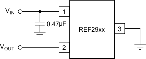 Figure 29. Typical Connections for Operating REF29xx
9.2 Typical Application
Figure 30 shows a low-power reference and conditioning circuit. This circuit attenuates and level-shifts a bipolar input voltage within the proper input range of a single-supply low-power 16-bit ΔΣ ADC, such as the one inside the MSP430 or other similar single-supply ADCs. Precision reference circuits are used to level-shift the input signal, provide the ADC reference voltage and to create a well-regulated supply voltage for the low-power analog circuitry. A low-power, zero-drift, operational amplifier circuit is used to attenuate and level-shift the input signal.
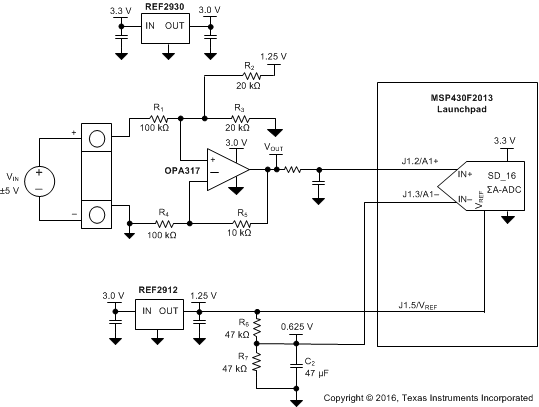 Figure 30. Low-Power Reference and Bipolar Voltage Conditioning Circuit for Low-Power ADCs
9.2.1 Design Requirements
- Supply Voltage: 3.3 V
- Maximum Input Voltage: ±6 V
- Specified Input Voltage: ±5 V
- ADC Reference Voltage: 1.25 V
The goal for this design is to accurately condition a ±5-V bipolar input voltage into a voltage suitable for conversion by a low-voltage ADC with a 1.25-V reference voltage, VREF, and an input voltage range of VREF / 2. The circuit should function with reduced performance over a wider input range of at least ±6 V to allow for easier protection of overvoltage conditions.
9.2.2 Detailed Design Procedure
Figure 30 depicts a simplified schematic for this design showing the MSP430 ADC inputs and full input-conditioning circuitry. The ADC is configured for a bipolar measurement where final conversion result is the differential voltage between the voltage at the positive and negative ADC inputs. The bipolar, GND referenced input signal must be level-shifted and attenuated by the operational amplifier so that the output is biased to VREF / 2 and has a differential voltage that is within the ±VREF / 2 input range of the ADC.
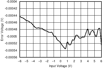
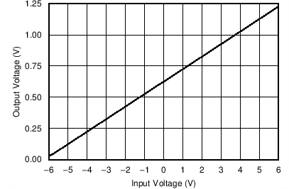
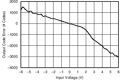
9.2.3 Application Curves
