SBAS452A September 2008 – January 2016 PCM3168A
PRODUCTION DATA.
- 1 Features
- 2 Applications
- 3 Description
- 4 Revision History
- 5 Description (continued)
- 6 Device Comparison Table
- 7 Pin Configuration and Functions
-
8 Specifications
- 8.1 Absolute Maximum Ratings
- 8.2 ESD Ratings
- 8.3 Recommended Operating Conditions
- 8.4 Thermal Information
- 8.5 Electrical Characteristics
- 8.6 Timing Requirements: System Clock
- 8.7 Timing Requirements: Power-On Reset
- 8.8 Timing Requirements: Audio Interface for Left-Justified, Right-Justified, and I2S (Slave Mode)
- 8.9 Timing Requirements: Audio Interface for Left-Justified, Right-Justified, and I2S (Master Mode)
- 8.10 Timing Requirements: Audio Interface for DSP and TDM (Slave Mode)
- 8.11 Timing Requirements: Audio Interface for DSP and TDM (Master Mode)
- 8.12 Timing Requirements: DAC Outputs and ADC Outputs
- 8.13 Timing Requirements: Four-Wire Serial Control Interface
- 8.14 Timing Requirements: SCL and SDA Control Interface
- 8.15 Typical Characteristics
-
9 Detailed Description
- 9.1 Overview
- 9.2 Functional Block Diagram
- 9.3
Feature Description
- 9.3.1 Analog Inputs
- 9.3.2 Analog Outputs
- 9.3.3 Voltage References
- 9.3.4 System Clock Input
- 9.3.5 Sampling Mode
- 9.3.6 Reset Operation
- 9.3.7 Highpass Filter (HPF)
- 9.3.8 Overflow Flag
- 9.3.9 Zero Flag
- 9.3.10 Four-Wire (SPI) Serial Control
- 9.3.11 Control Data Word Format
- 9.3.12 Register Write Operation
- 9.3.13 Register Read Operation
- 9.3.14 Two-Wire (I2C) Serial Control
- 9.3.15 Packet Protocol
- 9.3.16 Write Operation
- 9.3.17 Read Operation
- 9.4 Device Functional Modes
- 9.5 Register Maps
- 10Application and Implementation
- 11Power Supply Recommendations
-
12Layout
- 12.1
Layout Guidelines
- 12.1.1 Power-Supply Pins (VCCAD1/2, VCCDA1/2, and VDD1/2)
- 12.1.2 Grounding (AGNDAD1/2, AGNDDA1/2, and DGND1/2)
- 12.1.3 VIN1±, VIN2±, VIN3±, VIN4±, VIN5±, and VIN6± Pins
- 12.1.4 VCOMAD and VCOMDA Pins
- 12.1.5 VREFAD1/2 Pins
- 12.1.6 VOUT1±, VOU2±, VOUT3±, VOUT4±, VOUT5±, VOUT6±, VOUT7±, and VOUT8± Pins
- 12.1.7 MODE Pin
- 12.1.8 RST Pin
- 12.1.9 OVF Pin
- 12.1.10 System Clock and Audio Interface Clocks
- 12.1.11 PowerPAD
- 12.1.12 External Mute Control
- 12.2 Layout Example
- 12.1
Layout Guidelines
- 13Device and Documentation Support
- 14Mechanical, Packaging, and Orderable Information
8 Specifications
8.1 Absolute Maximum Ratings
over operating free-air temperature range (unless otherwise noted).(1)| MIN | MAX | UNIT | |||
|---|---|---|---|---|---|
| Supply voltage | VCCAD1 | –0.3 | 6.5 | V | |
| VCCAD2 | –0.3 | 6.5 | |||
| VCCDA1 | –0.3 | 6.5 | |||
| VCCDA2 | –0.3 | 6.5 | |||
| VDD1 | –0.3 | 4 | |||
| VDD2 | –0.3 | 4 | |||
| Ground voltage differences | AGNDAD1 | –0.1 | 0.1 | V | |
| AGNDAD2 | –0.1 | 0.1 | |||
| AGNDDA1 | –0.1 | 0.1 | |||
| AGNDDA2 | –0.1 | 0.1 | |||
| DGND1 | –0.1 | 0.1 | |||
| DGND2 | –0.1 | 0.1 | |||
| Supply voltage differences | VCCAD1 | –0.1 | 0.1 | V | |
| VCCAD2 | –0.1 | 0.1 | |||
| VCCDA1 | –0.1 | 0.1 | |||
| VCCDA2 | –0.1 | 0.1 | |||
| VDD1 | –0.1 | 0.1 | |||
| VDD2 | –0.1 | 0.1 | |||
| Digital input voltage | RST | –0.3 | 6.5 | V | |
| MS | –0.3 | 6.5 | |||
| MC | –0.3 | 6.5 | |||
| MDI | –0.3 | 6.5 | |||
| SCK | –0.3 | 6.5 | |||
| BCKAD/DA | –0.3 | (VDD + 0.3) < +4.0 | |||
| LRCKAD/DA | –0.3 | (VDD + 0.3) < +4.0 | |||
| DIN1/2/3/4 | –0.3 | (VDD + 0.3) < +4.0 | |||
| DOUT1/2/3 | –0.3 | (VDD + 0.3) < +4.0 | |||
| MODE | –0.3 | (VDD + 0.3) < +4.0 | |||
| OVF | –0.3 | (VDD + 0.3) < +4.0 | |||
| ZERO | –0.3 | (VDD + 0.3) < +4.0 | |||
| MDO | –0.3 | (VDD + 0.3) < +4.0 | |||
| Analog input voltage | VIN1-6± | –0.3 | (VCC + 0.3) < +6.5 | V | |
| VCOMAD/DA | –0.3 | (VCC + 0.3) < +6.5 | |||
| VOUT1-8± | –0.3 | (VCC + 0.3) < +6.5 | |||
| VREFAD1/2 | –0.3 | (VCC + 0.3) < +6.5 | |||
| Input current (all pins except supplies) | –10 | 10 | mA | ||
| Ambient temperature range (under bias) | –40 | 125 | °C | ||
| Junction temperature | 150 | °C | |||
| Lead temperature (soldering, 5s) | 260 | °C | |||
| Package temperature (IR reflow, peak) | 260 | °C | |||
| Storage temperature, Tstg | –55 | 150 | °C | ||
(1) Stresses beyond those listed under Absolute Maximum Ratings may cause permanent damage to the device. These are stress ratings only, which do not imply functional operation of the device at these or any other conditions beyond those indicated under Recommended Operating Conditions. Exposure to absolute-maximum-rated conditions for extended periods may affect device reliability.
8.2 ESD Ratings
| VALUE | UNIT | |||
|---|---|---|---|---|
| V(ESD) | Electrostatic discharge | Human body model (HBM), per ANSI/ESDA/JEDEC JS-001(1) | ±4000 | V |
| Charged-device model (CDM), per JEDEC specification JESD22-C101(2) | ±750 | |||
(1) JEDEC document JEP155 states that 500-V HBM allows safe manufacturing with a standard ESD control process.
(2) JEDEC document JEP157 states that 250-V CDM allows safe manufacturing with a standard ESD control process.
8.3 Recommended Operating Conditions
over operating free-air temperature range (unless otherwise noted).| MIN | NOM | MAX | UNIT | |||
|---|---|---|---|---|---|---|
| VCC | Analog supply voltage | 4.5 | 5.0 | 5.5 | V | |
| VDD | Digital supply voltage | 3.0 | 3.3 | 3.6 | V | |
| Digital Interface | LVTTL compatible | |||||
| Digital input clock frequency | Sampling frequency, LRCKAD/LRCKDA(1) | 8 | 96/192(1) | kHz | ||
| System clock frequency, SCKI | 2.048 | 36.864 | MHz | |||
| VI | Analog input level | Single-ended | 1 | VRMS | ||
| Differential | 2 | VRMS | ||||
| VO | Analog output voltage | Differential | 8 | VPP | ||
| VOLR | Analog output load resistance | To AC-coupled GND | 5 | kΩ | ||
| To DC-coupled GND | 15 | kΩ | ||||
| VOLC | Analog output load capacitance | 50 | pF | |||
| DOLC | Digital output load capacitance | 20 | pF | |||
| TA | Operating free-air temperature | PCM3168A Consumer grade | –40 | 25 | 85 | °C |
(1) 192 kHz is supported only for DAC.
8.4 Thermal Information
| THERMAL METRIC(1) | PCM3168A | UNIT | |
|---|---|---|---|
| PAP (HTQFP) | |||
| 64 PINS | |||
| RθJA | Junction-to-ambient thermal resistance | 26.1 | °C/W |
| RθJC(top) | Junction-to-case (top) thermal resistance | 7.7 | °C/W |
| RθJB | Junction-to-board thermal resistance | 8.9 | °C/W |
| ψJT | Junction-to-top characterization parameter | 0.2 | °C/W |
| ψJB | Junction-to-board characterization parameter | 8.7 | °C/W |
| RθJC(bot) | Junction-to-case (bottom) thermal resistance | 0.2 | °C/W |
(1) For more information about traditional and new thermal metrics, see the Semiconductor and IC Package Thermal Metrics application report, SPRA953.
8.5 Electrical Characteristics
At TA = 25°C, VCCAD1 = VCCAD2 = VCCDA1 = VCCDA2 = 5 V, VDD1 = VDD2 = 3.3 V, fS = 48 kHz, SCKI = 512 fS, 24-bit data, Sampling Mode = Auto for ADC and DAC, and Interface Mode = Slave for ADC and DAC, unless otherwise noted.| PARAMETER | TEST CONDITIONS | MIN | TYP | MAX | UNIT | |
|---|---|---|---|---|---|---|
| DATA FORMAT | ||||||
| Audio data interface format | I2S, LJ, RJ, DSP, TDM | |||||
| Audio data word length | 16, 24 | Bits | ||||
| Audio data format | MSB first, twos complement | |||||
| fS | Sampling frequency, ADC | 8 | 48 | 96 | kHz | |
| fS | Sampling frequency, DAC | 8 | 48 | 192 | kHz | |
| System clock frequency | 128 fS, 192 fS, 256 fS, 384 fS, 512 fS, 768 fS |
2.048 | 36.864 | MHz | ||
| INPUT LOGIC | ||||||
| VIH(1)(2) | Input logic level | 2 | VDD | VDC | ||
| VIL(1)(2) | 0.8 | |||||
| VIH(3)(4) | Input logic level | 2 | 5.5 | VDC | ||
| VIL(3)(4) | 0.8 | |||||
| IIH(2)(3) | Input logic level | VIN = VDD | ±10 | μA | ||
| IIL(2)(3) | VIN = 0 V | ±10 | ||||
| IIH(1)(4) | Input logic level | VIN = VDD | 65 | 100 | μA | |
| IIL(1)(4) | VIN = 0 V | ±10 | ||||
| OUTPUT LOGIC | ||||||
| VOH(5) | Output logic level | IOUT = –4 mA | 2.4 | VDC | ||
| VOL(5)(6) | IOUT = 4 mA | 0.4 | ||||
| REFERENCE INPUT/OUTPUT | ||||||
| VREFAD1 output voltage | VCCAD1 | V | ||||
| VREFAD2 output voltage | AGNDAD1 | V | ||||
| VCOMAD output voltage | 0.5 × VCCAD1 | V | ||||
| VCOMAD output impedance | 10 | kΩ | ||||
| Allowable VCOMAD output source/sink current | 1 | μA | ||||
| VCOMDA output voltage | 0.5 × VCCDA1 | V | ||||
| VCOMDA output impedance | 7.5 | kΩ | ||||
| Allowable VCOMDA output source/sink current | 1 | μA | ||||
| ADC CHARACTERISTICS | ||||||
| Resolution | 16 | 24 | Bits | |||
| Full-scale input voltage | VIN = 0 dB, Single-ended | 0.2 × VCCAD1 | VRMS | |||
| VIN = 0 dB, Differential | 0.4 × VCCAD1 | VRMS | ||||
| Center voltage | 0.5 × VCCAD1 | V | ||||
| Input impedance | 45 | kΩ | ||||
| Common-mode rejection ratio | 80 | dB | ||||
| DC ACCURACY | ||||||
| Gain mismatch channel-to-channel | Full-scale input, VIN | ±2.0 | ±6 | % of FSR | ||
| Gain error | Full-scale input, VIN | ±2.0 | ±6 | % of FSR | ||
| Bipolar zero error | Highpass filter bypass, VIN | ±1.0 | % of FSR | |||
| DYNAMIC PERFORMANCE(7)(8) | ||||||
| THD+N, VIN = –1 dB | fS = 48 kHz, Differential | –93 | –87 | dB | ||
| fS = 96 kHz, Differential | –93 | |||||
| fS = 48 kHz, Single-ended | –93 | |||||
| fS = 96 kHz, Single-ended | –93 | |||||
| Dynamic range | fS = 48 kHz, A-weighted, differential | 100 | 107 | dB | ||
| fS = 96 kHz, A-weighted, differential | 107 | |||||
| fS = 48 kHz, A-weighted, single-ended | 104 | |||||
| fS = 96 kHz, A-weighted, single-ended | 104 | |||||
| S/N ratio | fS = 48 kHz, A-weighted, differential | 100 | 107 | dB | ||
| fS = 96 kHz, A-weighted, differential | 107 | |||||
| fS = 48 kHz, A-weighted, single-ended | 104 | |||||
| fS = 96 kHz, A-weighted, single-ended | 104 | |||||
| Channel separation (between one channel and others) |
fS = 48 kHz, Differential | 98 | 104 | dB | ||
| fS = 96 kHz, Differential | 104 | |||||
| fS = 48 kHz, Single-ended | 101 | |||||
| fS = 96 kHz, Single-ended | 101 | |||||
| DIGITAL FILTER PERFORMANCE | ||||||
| Passband (single) | 0.454 × fS | Hz | ||||
| Passband (dual) | 0.454 × fS | Hz | ||||
| Stop band (single) | 0.555 × fS | Hz | ||||
| Stop band (dual) | 0.597 × fS | Hz | ||||
| Passband ripple | < 0.454 × fS, 0.454 × fS | ±0.035 | dB | |||
| Stop band attenuation | > 0.555 × fS, 0.597 × fS | –75 | dB | |||
| Group delay time (single) | 27 / fS | sec | ||||
| Group delay time (dual) | 17 / fS | sec | ||||
| Highpass filter frequency response | –3 dB | 0.02 × fS / 1000 | Hz | |||
| DAC CHARACTERISTICS | ||||||
| Resolution | 16 | 24 | Bits | |||
| DC ACCURACY | ||||||
| Gain mismatch channel-to-channel | ±2.0 | ±6 | % of FSR | |||
| Gain error | ±2.0 | ±6 | % of FSR | |||
| Bipolar zero error | ±1.0 | % of FSR | ||||
| DYNAMIC PERFORMANCE(9)(10) | ||||||
| THD+N, VOUT = 0 dB | fS = 48 kHz | –94 | –88 | dB | ||
| fS = 96 kHz | –94 | |||||
| fS = 192 kHz | –94 | |||||
| Dynamic range | fS = 48 kHz, EIAJ, A-weighted | 105 | 112 | dB | ||
| fS = 96 kHz, EIAJ, A-weighted | 112 | |||||
| fS = 192 kHz, EIAJ, A-weighted | 112 | |||||
| S/N ratio | fS = 48 kHz, EIAJ, A-weighted | 105 | 112 | dB | ||
| fS = 96 kHz, EIAJ, A-weighted | 112 | |||||
| fS = 192 kHz, EIAJ, A-weighted | 112 | |||||
| Channel separation (between one channel and others) |
fS = 48 kHz | 102 | 108 | dB | ||
| fS = 96 kHz | 108 | |||||
| fS = 192 kHz | 108 | |||||
| ANALOG OUTPUT | ||||||
| Output voltage | Differential | 1.6 × VCCDA1 | VPP | |||
| Center voltage | 0.5 × VCCDA1 | V | ||||
| Load impedance | To AC-coupled GND(11) | 5 | kΩ | |||
| To DC-coupled GND(11) | 15 | |||||
| Lowpass filter frequency response | f = 20 kHz | –0.04 | dB | |||
| f = 44 kHz | –0.18 | |||||
| DIGITAL FILTER PERFORMANCE(12) | Slow roll-off | |||||
| Passband (single, dual) | 0.454 × fS | Hz | ||||
| Passband (quad) | 0.432 × fS | Hz | ||||
| Stop band (single, dual) | 0.546 × fS | Hz | ||||
| Stop band (quad) | 0.569 × fS | Hz | ||||
| Passband ripple | ≤ 0.454 × fS | ±0.0018 | dB | |||
| Stop band attenuation | > 0.546 × fS, 0.569 × fS | –75 | dB | |||
| DIGITAL FILTER PERFORMANCE | Slow roll-off | |||||
| Passband | 0.328 × fS | Hz | ||||
| Stop band | 0.673 × fS | Hz | ||||
| Passband ripple | < 0.328 × fS | ±0.0013 | dB | |||
| Stop band attenuation | > 0.673 × fS | –75 | dB | |||
| DIGITAL FILTER PERFORMANCE(12) | ||||||
| Group delay time (single, dual) | 28/fS | sec | ||||
| Group delay time (quad) | 19/fS | sec | ||||
| De-emphasis error | ±0.1 | dB | ||||
| POWER-SUPPLY REQUIREMENTS | ||||||
| VCCxx1/2 | Voltage range | 4.5 | 5.0 | 5.5 | VDC | |
| VDD1/2 | 3.0 | 3.3 | 3.6 | |||
| ICC | Supply current | fS = 48 kHz/ADC, fS = 48 kHz/DAC | 162 | 210 | mA | |
| fS = 96 kHz/ADC, fS = 192 kHz/DAC | 162 | mA | ||||
| Full power-down(13) | 300 | μA | ||||
| IDD | fS = 48 kHz/ADC, fS = 48 kHz/DAC | 106 | 130 | mA | ||
| fS = 96 kHz/ADC, fS = 192 kHz/DAC | 127 | mA | ||||
| Full power-down(13) | 50 | μA | ||||
| Power dissipation | fS = 48 kHz/ADC, fS = 48 kHz/DAC | 1160 | 1480 | mW | ||
| fS = 96 kHz/ADC, fS = 192 kHz/DAC | 1230 | |||||
| fS = 48 kHz/ADC, Power-down/DAC | 660 | |||||
| Power-down/ADC, fS = 48 kHz/DAC | 633 | |||||
| Full power-down(13) | 1.67 | |||||
| TEMPERATURE RANGE | ||||||
| Operating temperature | PCM3168A Consumer grade | –40 | 85 | °C | ||
| θJA | Thermal resistance | HTQFP-64 | 21 | °C/W | ||
(1) BCKAD, BCKDA, LRCKAD, and LRCKDA (in slave mode, Schmitt trigger input with 50-kΩ typical internal pulldown resistor).
(2) DIN1/2/3/4 and MDO/ADR1/MD1. (Except SPI mode, Schmitt trigger input).
(3) SCKI, MDI/SDA/DEMP, and MC/SCL/FMT (Schmitt trigger input, 5-V tolerant).
(4) RST and MS/ADR0/MD0 (Schmitt trigger input with 50-kΩ typical internal pulldown resistor, 5-V tolerant).
(5) BCKAD, BCKDA, LRCKAD, and LRCKDA (in master mode), DOUT1/2/3, ZERO, OVF, and MDO/ADR1/MD1 (in SPI mode).
(6) SDA (in I2C mode, open-drain low output).
(7) In differential mode at VINx± pin, fIN = 1 kHz, using Audio Precision System II, RMS mode with 20-kHz lowpass filter and 400-Hz highpass filter.
(8) fS = 48 kHz : SCKI = 512 fS (single), fS = 96 kHz : SCKI = 256 fS (dual), fS = 192 kHz : SCKI = 128 fS (quad).
(9) In differential mode at VOUTx± pin, fOUT = 1 kHz, using Audio Precision System II, RMS mode with 20-kHz lowpass filter and 400-Hz highpass filter.
(10) fS = 48 kHz : SCKI = 512 fS (single), fS = 96 kHz : SCKI = 256 fS (dual), fS = 192 kHz : SCKI = 128 fS (quad).
(11) Allowable minimum input resistance of differential to single-ended converter with D to S Gain = G is calculated as (1 + 2G)/(1 + G) × 5k for AC-coupled and (1+ 0.9G)/(1 + G) × 15k for DC-coupled connection, refer to Figure 61 and Figure 62 of the Application Information section.
(12) Exclude single and dual at 128 fS, 192 fS system clock and quad at 256 fS to 768 fS system clock, and specifications for quad, single, and dual are respectively applied in reverse for them.
(13) Halt SCKI, BCKAD, BCKDA, LRCKAD, and LRCKDA.
8.6 Timing Requirements: System Clock
Refer to Figure 1.| MIN | MAX | UNIT | ||
|---|---|---|---|---|
| tSCY | System clock pulse cycle time | 27 | ns | |
| tSCH | System clock pulse width high | 10 | ns | |
| tSCL | System clock pulse width low | 10 | ns | |
| tDTY | System clock pulse duty cycle | 40% | 60% | |
8.7 Timing Requirements: Power-On Reset
Refer to Figure 2.| SINGLE | DUAL | QUAD | UNIT | ||
|---|---|---|---|---|---|
| tDACDLY1 | DAC delay time internal reset release to VOUT start | 3600 | 7200 | 14400 | Period of LRCKDA |
| tDACDLY2 | DAC fade-in/fade-out time | 2048 | 4096 | 8192 | Period of LRCKDA |
| tADCDLY1 | ADC delay time internal reset release to DOUT start | 4800 | 9600 | N/A | Period of LRCKAD |
| tADCDLY2 | ADC fade-in/fade-out time | 2048 | 4096 | N/A | Period of LRCKAD |
8.8 Timing Requirements: Audio Interface for Left-Justified, Right-Justified, and I2S (Slave Mode)(1)
Refer to Figure 3.| MIN | NOM | MAX | UNIT | ||
|---|---|---|---|---|---|
| tBCY | BCKAD/DA cycle time | 75 | ns | ||
| tBCH | BCKAD/DA pulse width high | 35 | ns | ||
| tBCL | BCKAD/DA pulse width low | 35 | ns | ||
| tLRS | LRCKAD/DA setup time to BCKAD/DA rising edge | 10 | ns | ||
| tLRH | LRCKAD/DA hold time to BCKAD/DA rising edge | 10 | ns | ||
| tDIS | DIN1/2/3/4 setup time to BCKDA rising edge | 10 | ns | ||
| tDIH | DIN1/2/3/4 hold time to BCKDA rising edge | 10 | ns | ||
| tDOD | DOUT1/2/3 delay time from BCKAD falling edge | 0 | 30 | ns | |
(1) Load capacitance of output is 20 pF.
8.9 Timing Requirements: Audio Interface for Left-Justified, Right-Justified, and I2S (Master Mode)(1)
Refer to Figure 4.| MIN | TYP | MAX | UNIT | ||
|---|---|---|---|---|---|
| tBCY | BCKAD/DA cycle time | 1 / (64 × fS) | |||
| tBCH | BCKAD/DA pulse width high | 0.4 × tBCY | 0.5 × tBCY | 0.6 × tBCY | |
| tBCL | BCKAD/DA pulse width low | 0.4 × tBCY | 0.5 × tBCY | 0.6 × tBCY | |
| tLRD | LRCKAD/DA delay time from BCKAD/DA falling edge | –10 | 20 | ns | |
| tDIS | DIN1/2/3/4 setup time to BCKDA rising edge | 10 | ns | ||
| tDIH | DIN1/2/3/4 hold time to BCKDA rising edge | 10 | ns | ||
| tDOD | DOUT1/2/3 delay time from BCKAD falling edge | –10 | 20 | ns | |
(1) Load capacitance of output is 20 pF.
8.10 Timing Requirements: Audio Interface for DSP and TDM (Slave Mode)(1)
Refer to Figure 5.| MIN | TYP | MAX | UNIT | ||
|---|---|---|---|---|---|
| tBCY | BCKAD cycle time | 75 | ns | ||
| BCKDA cycle time | 40 | ns | |||
| tBCH | BCKAD pulse width high | 35 | ns | ||
| BCKDA pulse width high | 15 | ns | |||
| tBCL | BCKAD pulse width low | 35 | ns | ||
| BCKDA pulse width low | 15 | ns | |||
| tLRW | LRCKAD/DA pulse width high (DSP format) | tBCY | |||
| LRCKAD/DA pulse width high (TDM format) | tBCY | 1 / fS – tBCY | |||
| tLRS | LRCKAD/DA setup time to BCKAD/DA rising edge | 10 | ns | ||
| tLRH | LRCKAD/DA hold time to BCKAD/DA rising edge | 10 | ns | ||
| tDIS | DIN1/2/3/4 setup time to BCKDA rising edge | 10 | ns | ||
| tDIH | DIN1/2/3/4 hold time to BCKDA rising edge | 10 | ns | ||
| tDOD | DOUT1/2/3 delay time from BCKAD falling edge | 0 | 30 | ns | |
(1) Load capacitance of output is 20 pF.
8.11 Timing Requirements: Audio Interface for DSP and TDM (Master Mode)(1)
Refer to Figure 6.| MIN | TYP | MAX | UNIT | ||
|---|---|---|---|---|---|
| tBCY | BCKAD/DA cycle time (DSP format) | 1 / (64 × fS) | |||
| BCKAD/DA cycle time (TDM format, single rate) | 1 / (256 × fS) | ||||
| BCKAD/DA cycle time (TDM format, dual rate) | 1 / (128 × fS) | ||||
| tBCH | BCKAD/DA pulse width high | 0.4 × tBCY | 0.5 × tBCY | 0.6 × tBCY | |
| tBCL | BCKAD/DA pulse width low | 0.4 × tBCY | 0.5 × tBCY | 0.6 × tBCY | |
| tLRW | LRCKAD/DA pulse width high (DSP format) | tBCY | |||
| LRCKAD/DA pulse width high (TDM format) | 1 / (2 × fS) | ||||
| tLRD | LRCKAD/DA delay time from BCKAD/DA falling edge | –10 | 20 | ns | |
| tDIS | DIN1/2/3/4 setup time to BCKDA rising edge | 10 | ns | ||
| tDIH | DIN1/2/3/4 hold time to BCKDA rising edge | 10 | ns | ||
| tDOD | DOUT1/2/3 delay time from BCKAD falling edge | –10 | 20 | ns | |
(1) Load capacitance of output is 20 pF.
8.12 Timing Requirements: DAC Outputs and ADC Outputs
Refer to Figure 7.| SINGLE | DUAL | QUAD | UNIT | ||
|---|---|---|---|---|---|
| tDACDLY3 | DAC delay synchronization detect to normal data | 38 | 38 | 29 | Period of LRCKDA |
| tADCDLY3 | ADC delay synchronization detect to normal data | 60 | 60 | N/A | Period of LRCKAD |
8.13 Timing Requirements: Four-Wire Serial Control Interface(1)
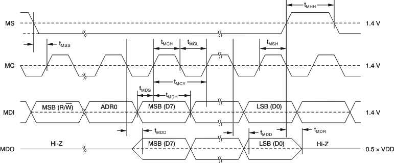
Refer to Figure 8.| MIN | MAX | UNIT | ||
|---|---|---|---|---|
| tMCY | MC pulse cycle time | 100 | ns | |
| tMCL | MC low-level time | 40 | ns | |
| tMCH | MC high-level time | 40 | ns | |
| tMHH | MS high-level time | tMCY | ns | |
| tMSS | MS falling edge to MC rising edge | 30 | ns | |
| tMSH | MS rising edge from MC rising edge for LSB | 15 | ns | |
| tMDH | MDI hold time | 15 | ns | |
| tMDS | MDI setup time | 15 | ns | |
| tMDD | MDO enable or delay time from MC falling edge | 0 | 30 | ns |
| tMDR | MDO disable time from MS rising edge | 0 | 30 | ns |
(1) These timing parameters are critical for proper control port operation.
8.14 Timing Requirements: SCL and SDA Control Interface
Refer to Figure 9.| STANDARD MODE | FAST MODE | UNIT | ||||
|---|---|---|---|---|---|---|
| MIN | MAX | MIN | MAX | |||
| fSCL | SCL clock frequency | 100 | 400 | kHz | ||
| tBUF | Bus free time between STOP and START condition | 4.7 | 1.3 | μs | ||
| tLOW | Low period of the SCL clock | 4.7 | 1.3 | μs | ||
| tHI | High period of the SCL clock | 4.0 | 0.6 | μs | ||
| tS-SU | Setup time for START/Repeated START condition | 4.7 | 0.6 | μs | ||
| tS-HD | Hold time for START/Repeated START condition | 4.0 | 0.6 | μs | ||
| tD-SU | Data setup time | 250 | 100 | ns | ||
| tD-HD | Data hold time | 0 | 3450 | 0 | 900 | ns |
| tSCL-R | Rise time of SCL signal | 1000 | 20 + (0.1 × CB) | 300 | ns | |
| tSCL-F | Fall time of SCL signal | 1000 | 20 + (0.1 × CB) | 300 | ns | |
| tSDA-R | Rise time of SDA signal | 1000 | 20 + (0.1 × CB) | 300 | ns | |
| tSDA-F | Fall time of SDA signal | 1000 | 20 + (0.1 × CB) | 300 | ns | |
| tP-SU | Setup time for STOP condition | 4.0 | 0.6 | μs | ||
| tGW | Allowable glitch width | N/A | 50 | |||
| CB | Capacitive load for SDA and SCL line | 400 | 100 | pF | ||
| VNH | Noise margin at high level for each connected device (including hysteresis) |
0.2 × VDD | 0.2 × VDD | V | ||
| VNL | Noise margin at low level for each connected device (including hysteresis) |
0.1 × VDD | 0.1 × VDD | V | ||
| VHYS | Hysteresis of Schmitt-trigger input | N/A | 0.05 × VDD | V | ||
 Figure 1. System Clock Timing Requirements
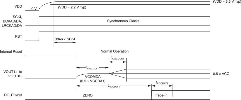 Figure 2. Power-On Reset Timing Requirements
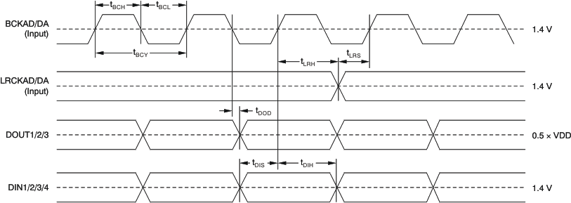 Figure 3. Audio Interface Timing Requirements for Left-Justified, Right-Justified, and I2S Data Formats (Slave Mode)
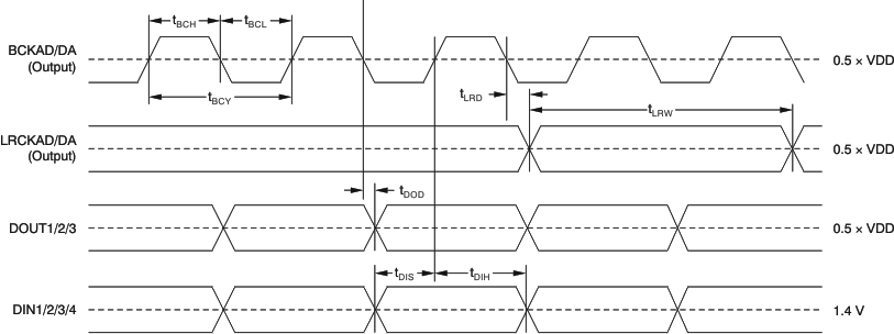 Figure 4. Audio Interface Timing Requirements for Left-Justified, Right-Justified, and I2S Data Formats (Master Mode)
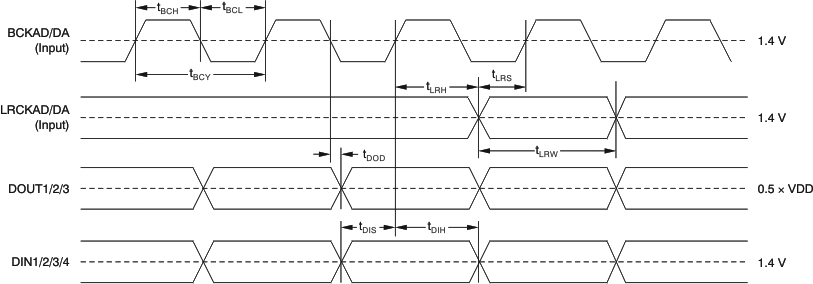 Figure 5. Audio Interface Timing Requirements for DSP and TDM Data Formats (Slave Mode)
 Figure 6. Audio Interface Timing Requirements for DSP and TDM Data Formats (Master Mode)
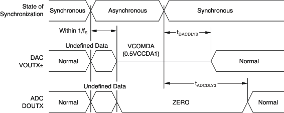 Figure 7. DAC Outputs and ADC Outputs for Loss of Synchronization
1.
Figure 8. Four-Wire Serial Control Interface Timing
NOINDENT:
These timing parameters are critical for proper control port operation. Figure 9. SCL and SDA Control Interface Timing
8.15 Typical Characteristics
8.15.1 ADC Digital Filter
At TA = 25°C, VCCAD1 = VCCAD2 = VCCDA1 = VCCDA2 = 5 V, VDD1 = VDD2 = 3.3 V, fS = 48 kHz, SCKI = 512 fS, 24-bit data, Sampling Mode = Auto for ADC and DAC, and Interface Mode = Slave for ADC and DAC, unless otherwise noted.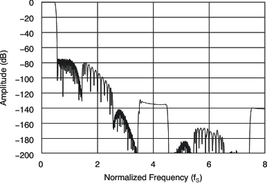 Figure 10. Frequency Response (Single Rate)
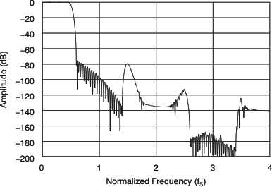 Figure 12. Frequency Response (Dual Rate)
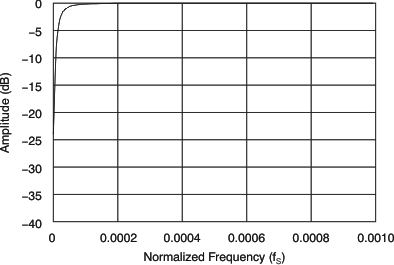 Figure 14. HPF Frequency Response
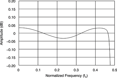 Figure 11. Frequency Response Passband (Single Rate)
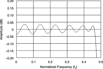 Figure 13. Frequency Response Passband (Dual Rate)
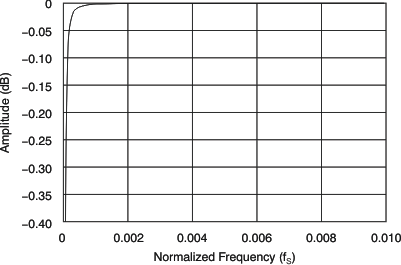 Figure 15. HPF Frequency Response Passband
8.15.2 DAC Digital Filter
At TA = 25°C, VCCAD1 = VCCAD2 = VCCDA1 = VCCDA2 = 5 V, VDD1 = VDD2 = 3.3 V, fS = 48 kHz, SCKI = 512 fS, 24-bit data, Sampling Mode = Auto for ADC and DAC, and Interface Mode = Slave for ADC and DAC, unless otherwise noted.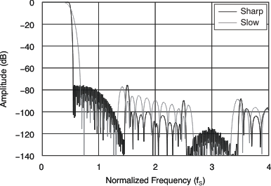 Figure 16. Frequency Response (Single Rate)
 Figure 18. Frequency Response (Dual Rate)
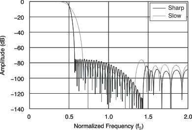 Figure 20. Frequency Response (Quad Rate)
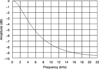 Figure 22. De-Emphasis Characteristic (FS = 48 kHz)
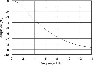 Figure 24. De-Emphasis Characteristic (FS = 32 kHz)
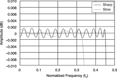 Figure 17. Frequency Response Passband (Single Rate)
 Figure 19. Frequency Response Passband (Dual Rate)
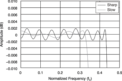 Figure 21. Frequency Response Passband (Quad Rate)
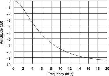 Figure 23. De-Emphasis Characteristic (FS = 44 kHz)
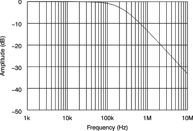 Figure 25. Analog Filter Characteristic
8.15.3 ADC Performance
At TA = 25°C, VCCAD1 = VCCAD2 = VCCDA1 = VCCDA2 = 5 V, VDD1 = VDD2 = 3.3 V, fS = 48 kHz, SCKI = 512 fS, 24-bit data, Sampling Mode = Auto for ADC and DAC, and Interface Mode = Slave for ADC and DAC, unless otherwise noted.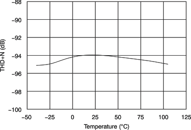 Figure 26. THD+N At –1 dB vs Temperature
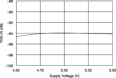 Figure 28. THD+N At –1 dB vs Supply Voltage
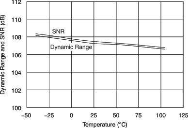 Figure 27. Dynamic Range and SNR vs Temperature
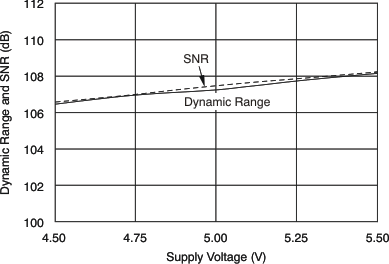 Figure 29. Dynamic Range and SNR vs Supply Voltage
8.15.4 DAC Performance
At TA = 25°C, VCCAD1 = VCCAD2 = VCCDA1 = VCCDA2 = 5 V, VDD1 = VDD2 = 3.3 V, fS = 48 kHz, SCKI = 512 fS, 24-bit data, Sampling Mode = Auto for ADC and DAC, and Interface Mode = Slave for ADC and DAC, unless otherwise noted.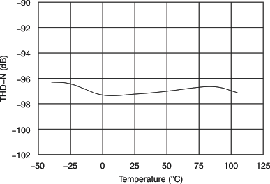 Figure 30. THD+N vs Temperature
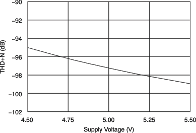 Figure 32. THD+N vs Supply Voltage
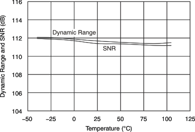 Figure 31. Dynamic Range and SNR vs Temperature
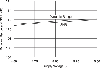 Figure 33. Dynamic Range and SNR vs Supply Voltage
8.15.5 Output Spectrum
At TA = 25°C, VCCAD1 = VCCAD2 = VCCDA1 = VCCDA2 = 5 V, VDD1 = VDD2 = 3.3 V, fS = 48 kHz, SCKI = 512 fS, 24-bit data, Sampling Mode = Auto for ADC and DAC, and Interface Mode = Slave for ADC and DAC, unless otherwise noted.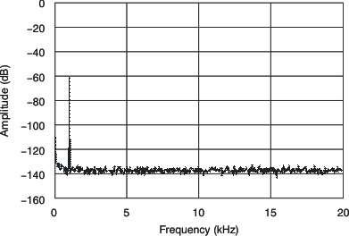 Figure 34. ADC Output Spectrum (–60 dB, N = 32768)
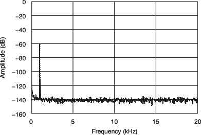 Figure 35. DAC Output Spectrum (–60 dB, N = 32768)
8.15.6 Power-Supply
At TA = 25°C, VCCAD1 = VCCAD2 = VCCDA1 = VCCDA2 = 5 V, VDD1 = VDD2 = 3.3 V, fS = 48 kHz, SCKI = 512 fS, 24-bit data, Sampling Mode = Auto for ADC and DAC, and Interface Mode = Slave for ADC and DAC, unless otherwise noted.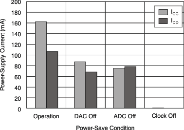 Figure 36. Power-Supply Current vs Power-Save Condition